

Lattice Semiconductor Corporation
LFE2-12SE-5Q208C
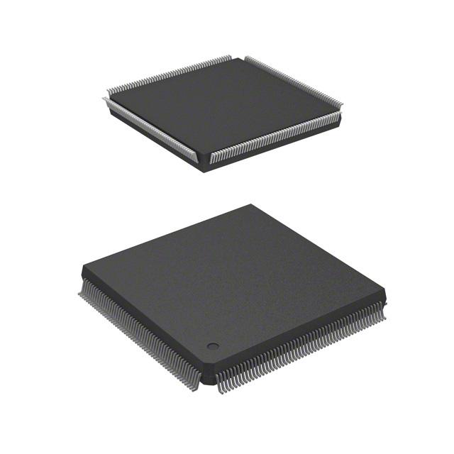
LFE2-12SE-5Q208C ECAD Model
LFE2-12SE-5Q208C Attributes
| Type | Description | Select |
|---|---|---|
| Mfr | Lattice Semiconductor Corporation | |
| Series | ECP2 | |
| Package | Tray | |
| Number of LABs/CLBs | 1500 | |
| Number of Logic Elements/Cells | 12000 | |
| Total RAM Bits | 226304 | |
| Number of I/O | 131 | |
| Voltage - Supply | 1.14V ~ 1.26V | |
| Mounting Type | Surface Mount | |
| Operating Temperature | 0°C ~ 85°C (TJ) | |
| Package / Case | 208-BFQFP | |
| Supplier Device Package | 208-PQFP (28x28) | |
| Base Product Number | LFE2-12 |
LFE2-12SE-5Q208C Datasheet Download
LFE2-12SE-5Q208C Overview
The LFE2-12SE-5Q208C chip model is a low-power, low-cost, low-footprint FPGA (Field Programmable Gate Array) designed by Lattice Semiconductor. It is based on the LatticeECP2M architecture and is optimized for low-power applications.
The LFE2-12SE-5Q208C is a low-cost, low-power, low-footprint FPGA with a total of 12,288 logic elements, including 5,208 configurable logic blocks (CLBs). It also has up to 192Kbits of embedded RAM, up to 24 DSP slices, and two PLLs for clock management. It has a maximum operating frequency of up to 250MHz and a maximum I/O pin count of up to 622. The device also supports up to 8 user-defined I/O standards and up to 32 LVDS pairs. It also has a wide range of power management features, such as power-down, clock gating and dynamic power scaling.
The LFE2-12SE-5Q208C is ideal for applications such as consumer electronics, industrial automation, medical, automotive, and aerospace. It is suitable for a wide range of applications, including embedded vision, machine learning, and AI. It is also suitable for applications requiring low power, high performance, and low cost, such as IoT, wearables, and embedded systems.
You May Also Be Interested In

2,876 In Stock
Pricing (USD)
| QTY | Unit Price | Ext Price |
|---|---|---|
| No reference price found. | ||