
Lattice Semiconductor Corporation
LCMXO2280C-3TN144I
LCMXO2280C-3TN144I ECAD Model
LCMXO2280C-3TN144I Attributes
| Type | Description | Select |
|---|---|---|
| Mfr | Lattice Semiconductor Corporation | |
| Series | MachXO | |
| Package | Tray | |
| Number of LABs/CLBs | 285 | |
| Number of Logic Elements/Cells | 2280 | |
| Total RAM Bits | 28262 | |
| Number of I/O | 113 | |
| Voltage - Supply | 1.71V ~ 3.465V | |
| Mounting Type | Surface Mount | |
| Operating Temperature | -40°C ~ 100°C (TJ) | |
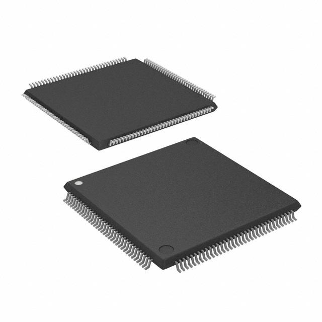
| Package / Case | 144-LQFP | |
| Supplier Device Package | 144-TQFP (20x20) | |
| Base Product Number | LCMXO2280 |
LCMXO2280C-3TN144I Datasheet Download
LCMXO2280C-3TN144I Overview
The LCMXO2280C-3TN144I is a low-cost, high-performance FPGA chip from Lattice Semiconductor Corporation. It is based on the Lattice CrossLink-NX FPGA architecture and is designed to provide high-speed, low-power performance in a small form factor. The chip features 144Kbits of memory, up to 854 user I/O pins, up to 100MHz of user clock frequency and up to 854 user I/O pins. It has a maximum operating voltage of 1.2V and a maximum power consumption of 1.2W.
The LCMXO2280C-3TN144I is ideal for applications requiring high-speed, low-power performance such as industrial automation, medical imaging, motor control, and automotive. It is well-suited for applications such as motor control, motion control, robotics, and embedded systems. It is also suitable for high-speed data acquisition, communications, and signal processing.
The chip is also equipped with a wide range of features such as a wide range of I/O standards, high-speed LVDS, LVCMOS, LVTTL, and HSTL, as well as high-speed differential I/O. It also features an integrated phase-locked loop (PLL) and a wide range of on-chip memories, including SRAM, Flash, and EEPROM. Additionally, the chip supports a wide range of high-speed serial transceivers, including PCIe, USB3.0, and SATA.
In summary, the LCMXO2280C-3TN144I is a low-cost, high-performance FPGA chip from Lattice Semiconductor Corporation. It is designed to provide high-speed, low-power performance in a small form factor, and is suitable for a wide range of applications such as industrial automation, medical imaging, motor control, and automotive. It is equipped with a wide range of features such as a wide range of I/O standards, high-speed LVDS, LVCMOS, LVTTL, and HSTL, as well as high-speed differential I/O. It also features an integrated phase-locked loop (PLL) and a wide range of on-chip memories, including SRAM, Flash, and EEPROM.
You May Also Be Interested In
3,058 In Stock
Pricing (USD)
| QTY | Unit Price | Ext Price |
|---|---|---|
| 1+ | $43.4648 | $43.4648 |
| 10+ | $42.9974 | $429.9740 |
| 100+ | $40.6606 | $4,066.0581 |
| 1000+ | $38.3238 | $19,161.8830 |
| 10000+ | $35.0522 | $35,052.2250 |
| The price is for reference only, please refer to the actual quotation! | ||