
Lattice Semiconductor Corporation
LCMXO2-640UHC-6TG144I
LCMXO2-640UHC-6TG144I ECAD Model
LCMXO2-640UHC-6TG144I Attributes
| Type | Description | Select |
|---|---|---|
| Mfr | Lattice Semiconductor Corporation | |
| Series | MachXO2 | |
| Package | Tray | |
| Number of LABs/CLBs | 80 | |
| Number of Logic Elements/Cells | 640 | |
| Total RAM Bits | 65536 | |
| Number of I/O | 107 | |
| Voltage - Supply | 2.375V ~ 3.465V | |
| Mounting Type | Surface Mount | |
| Operating Temperature | -40°C ~ 100°C (TJ) | |
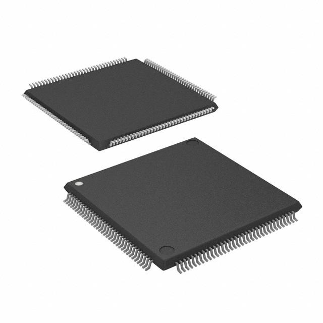
| Package / Case | 144-LQFP | |
| Supplier Device Package | 144-TQFP (20x20) | |
| Base Product Number | LCMXO2-640 |
LCMXO2-640UHC-6TG144I Datasheet Download
LCMXO2-640UHC-6TG144I Overview
The LCMXO2-640UHC-6TG144I is a Field Programmable Gate Array (FPGA) chip manufactured by Lattice Semiconductor Corporation. This chip is based on the LatticeECP2M family of FPGAs and is designed for low-cost, low-power applications. It features a 6-input Look-up Table (LUT) architecture, with a maximum of 640 logic cells and 144 I/O pins, and operates at a maximum speed of up to 300 MHz.
The chip is ideal for applications requiring high performance, low power consumption and low cost. It is suitable for a wide range of applications, including embedded systems, industrial control, medical equipment, consumer electronics, automotive systems and communications systems.
The LCMXO2-640UHC-6TG144I is available in a small, 1.4 mm x 1.4 mm, 144-pin TQFP package with 0.5 mm pin pitch. It has an operating temperature range of -40°C to 85°C and is RoHS compliant.
The chip also offers a wide range of features, such as high-speed clock frequency synthesis, high-speed transceivers, high-speed IO-banks, phase-locked loops, and programmable I/O voltage support. It also supports multiple power-saving modes, such as low power sleep mode, power-down mode and power-down suspend mode.
In addition, the chip includes a comprehensive design suite, including the Lattice Diamond design software, which provides an intuitive design environment, allowing designers to quickly and easily create FPGA designs. It also includes the Lattice IPexpress IP library, which provides an extensive library of pre-verified IP cores and design blocks.
Overall, the LCMXO2-640UHC-6TG144I is a cost-effective, low-power FPGA chip, suitable for a wide range of applications. It offers a high-performance, low-power solution for embedded, industrial, medical, consumer electronics, automotive and communications applications.
You May Also Be Interested In
4,690 In Stock
Pricing (USD)
| QTY | Unit Price | Ext Price |
|---|---|---|
| 1+ | $12.2873 | $12.2873 |
| 10+ | $12.1552 | $121.5522 |
| 100+ | $11.4946 | $1,149.4614 |
| 1000+ | $10.8340 | $5,417.0020 |
| 10000+ | $9.9092 | $9,909.1500 |
| The price is for reference only, please refer to the actual quotation! | ||