
Lattice Semiconductor Corporation
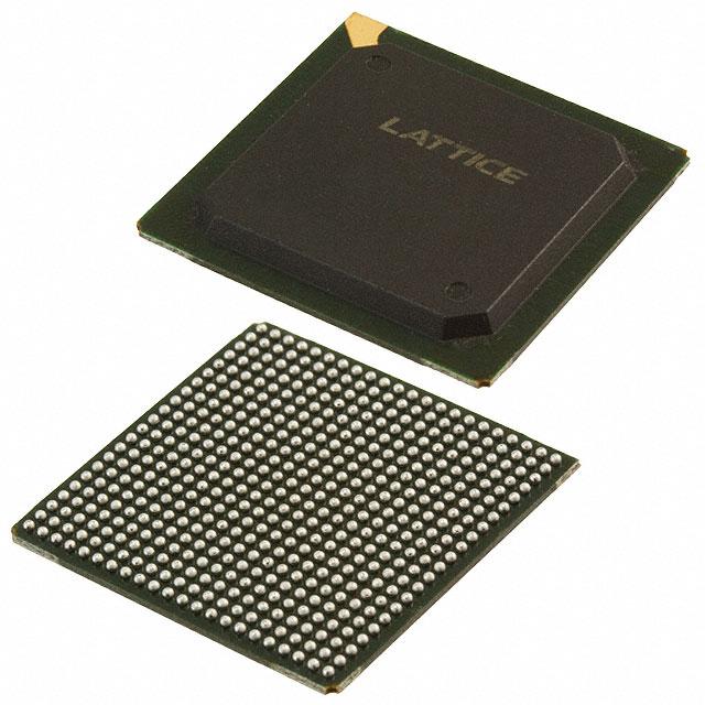
LCMXO2-4000HE-5FG484C
LCMXO2-4000HE-5FG484C ECAD Model
LCMXO2-4000HE-5FG484C Attributes
| Type | Description | Select |
|---|---|---|
| Mfr | Lattice Semiconductor Corporation | |
| Series | MachXO2 | |
| Package | Tray | |
| Number of LABs/CLBs | 540 | |
| Number of Logic Elements/Cells | 4320 | |
| Total RAM Bits | 94208 | |
| Number of I/O | 278 | |
| Voltage - Supply | 1.14V ~ 1.26V | |
| Mounting Type | Surface Mount | |
| Operating Temperature | 0°C ~ 85°C (TJ) | |
| Package / Case | 484-BBGA | |
| Supplier Device Package | 484-FBGA (23x23) | |
| Base Product Number | LCMXO2-4000 |
LCMXO2-4000HE-5FG484C Datasheet Download
LCMXO2-4000HE-5FG484C Overview
The LCMXO2-4000HE-5FG484C is a low-cost, high-performance, low-power Field Programmable Gate Array (FPGA) chip. It is based on the LatticeECP2M architecture and is fabricated using a 0.5um process. The chip features a total of 4,000 logic elements, 576 Kbits of embedded RAM, and 484 user-defined I/O pins. It also includes two dedicated clock management blocks and two dedicated phase-locked loop (PLL) blocks for clock and timing management.
The LCMXO2-4000HE-5FG484C is designed to be used in a wide variety of applications. It is ideal for embedded control, signal processing, and communications applications. It can also be used in data acquisition, motor control, and industrial automation applications. The chip has a maximum operating frequency of 400 MHz and a power dissipation of 1.2 W. It has a wide operating temperature range of -40°C to +85°C, making it suitable for both industrial and commercial applications.
The LCMXO2-4000HE-5FG484C is programmed using the Lattice Diamond design software. It supports the industry-standard JTAG boundary scan, as well as the proprietary Lattice ISP programming protocol. The chip is available in a 484-pin Fine Pitch Ball Grid Array (FBGA) package, making it suitable for high-density board designs. The chip is also RoHS compliant, making it a great choice for environmentally conscious designs.
You May Also Be Interested In
4,907 In Stock
Pricing (USD)
| QTY | Unit Price | Ext Price |
|---|---|---|
| 1+ | $23.7709 | $23.7709 |
| 10+ | $23.5153 | $235.1529 |
| 100+ | $22.2373 | $2,223.7287 |
| 1000+ | $20.9593 | $10,479.6410 |
| 10000+ | $19.1701 | $19,170.0750 |
| The price is for reference only, please refer to the actual quotation! | ||