
Lattice Semiconductor Corporation
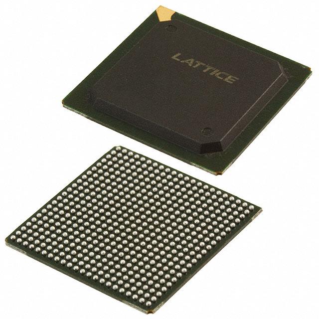
LCMXO2-2000UHC-5FG484C
LCMXO2-2000UHC-5FG484C ECAD Model
LCMXO2-2000UHC-5FG484C Attributes
| Type | Description | Select |
|---|---|---|
| Mfr | Lattice Semiconductor Corporation | |
| Series | MachXO2 | |
| Package | Tray | |
| Number of LABs/CLBs | 264 | |
| Number of Logic Elements/Cells | 2112 | |
| Total RAM Bits | 94208 | |
| Number of I/O | 278 | |
| Voltage - Supply | 2.375V ~ 3.465V | |
| Mounting Type | Surface Mount | |
| Operating Temperature | 0°C ~ 85°C (TJ) | |
| Package / Case | 484-BBGA | |
| Supplier Device Package | 484-FBGA (23x23) | |
| Base Product Number | LCMXO2-2000 |
LCMXO2-2000UHC-5FG484C Datasheet Download
LCMXO2-2000UHC-5FG484C Overview
The LCMXO2-2000UHC-5FG484C is a low-power, high-performance, field-programmable gate array (FPGA) chip, designed and manufactured by Lattice Semiconductor Corporation. This FPGA chip is based on the Lattice MachXO2 family of FPGAs and is offered in a small 5x5 mm, 484-pin FineLine BGA package. It has a maximum operating frequency of up to 200 MHz and a maximum I/O count of up to 144 I/Os.
The LCMXO2-2000UHC-5FG484C is designed for a wide range of applications, including industrial automation, consumer electronics, automotive, medical, and networking. It is suitable for applications requiring low-power, low-cost, and high-performance solutions. It features a low-power, low-noise, and low-EMI design, which provides an efficient and reliable solution for a wide range of applications.
The LCMXO2-2000UHC-5FG484C is a highly integrated FPGA chip that offers a wide range of features and benefits, including a wide range of I/O configurations, high-speed I/O, advanced memory and DSP blocks, and a wide range of configurable logic blocks. It also features an on-chip oscillator, programmable I/O voltage, and integrated flash memory. The chip also supports multiple I/O standards, including LVTTL, LVCMOS, and HSTL, as well as a wide range of clock management features.
In summary, the LCMXO2-2000UHC-5FG484C is a low-power, high-performance, field-programmable gate array (FPGA) chip, designed and manufactured by Lattice Semiconductor Corporation. It is suitable for a wide range of applications and offers a wide range of features and benefits, including a wide range of I/O configurations, high-speed I/O, advanced memory and DSP blocks, and a wide range of configurable logic blocks. It is an ideal choice for applications requiring low-power, low-cost, and high-performance solutions.
You May Also Be Interested In
4,913 In Stock
Pricing (USD)
| QTY | Unit Price | Ext Price |
|---|---|---|
| 1+ | $28.0770 | $28.0770 |
| 10+ | $27.7751 | $277.7508 |
| 100+ | $26.2656 | $2,626.5561 |
| 1000+ | $24.7560 | $12,378.0230 |
| 10000+ | $22.6427 | $22,642.7250 |
| The price is for reference only, please refer to the actual quotation! | ||