
Lattice Semiconductor Corporation
LCMXO2-2000HE-5TG100C
LCMXO2-2000HE-5TG100C ECAD Model
LCMXO2-2000HE-5TG100C Attributes
| Type | Description | Select |
|---|---|---|
| Mfr | Lattice Semiconductor Corporation | |
| Series | MachXO2 | |
| Package | Tray | |
| Number of LABs/CLBs | 264 | |
| Number of Logic Elements/Cells | 2112 | |
| Total RAM Bits | 75776 | |
| Number of I/O | 79 | |
| Voltage - Supply | 1.14V ~ 1.26V | |
| Mounting Type | Surface Mount | |
| Operating Temperature | 0°C ~ 85°C (TJ) | |
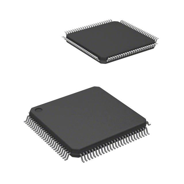
| Package / Case | 100-LQFP | |
| Supplier Device Package | 100-TQFP (14x14) | |
| Base Product Number | LCMXO2-2000 |
LCMXO2-2000HE-5TG100C Datasheet Download
LCMXO2-2000HE-5TG100C Overview
The LCMXO2-2000HE-5TG100C is a field-programmable gate array (FPGA) chip manufactured by Lattice Semiconductor. It is a low-cost, low-power, high-performance device that is suitable for a wide range of applications.
The LCMXO2-2000HE-5TG100C has a maximum operating frequency of up to 200 MHz and is built with a 5-layer metal process. It features a total of 1,000 logic cells, including 4-input look-up tables (LUTs) and flip-flops. It also has 10Kbits of embedded RAM and two dedicated clock management blocks. The device is packaged in a 5x5 mm, 100-pin TQFP package.
The LCMXO2-2000HE-5TG100C is ideal for applications that require low power consumption, high performance, and a low cost. It is suitable for applications such as industrial and consumer control, digital signal processing, and communication systems. It is also suitable for automotive and medical applications, as well as for applications that require low power and high performance.
In summary, the LCMXO2-2000HE-5TG100C is a low-cost, low-power, high-performance FPGA device that is suitable for a wide range of applications. It features a maximum operating frequency of up to 200 MHz, 1,000 logic cells, 10Kbits of embedded RAM, and two dedicated clock management blocks. It is packaged in a 5x5 mm, 100-pin TQFP package and is suitable for applications such as industrial and consumer control, digital signal processing, and communication systems.
You May Also Be Interested In

3,406 In Stock
Pricing (USD)
| QTY | Unit Price | Ext Price |
|---|---|---|
| 1+ | $9.7464 | $9.7464 |
| 10+ | $9.6416 | $96.4160 |
| 100+ | $9.1176 | $911.7600 |
| 1000+ | $8.5936 | $4,296.8000 |
| 10000+ | $7.8600 | $7,860.0000 |
| The price is for reference only, please refer to the actual quotation! | ||