
Lattice Semiconductor Corporation
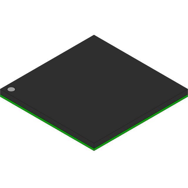
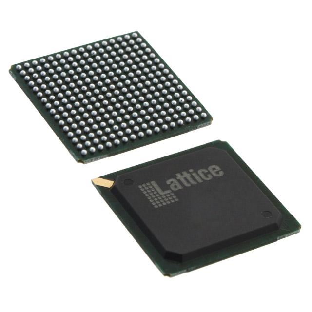
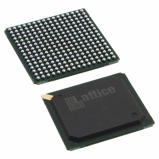
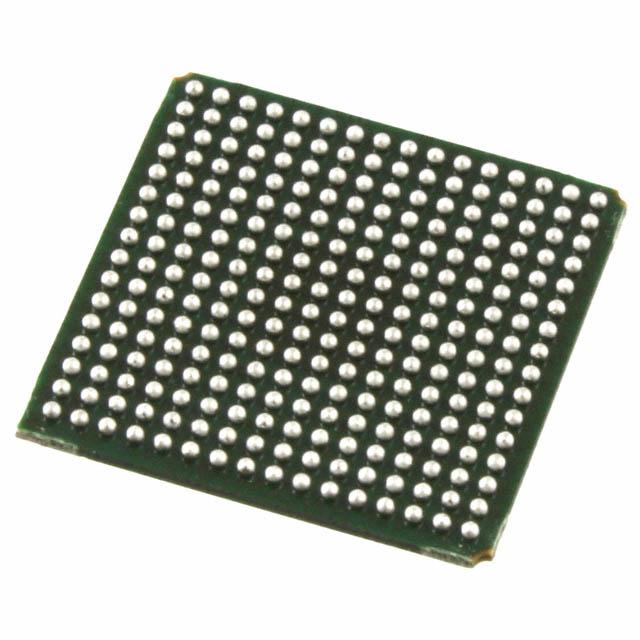
LC4256V-3F256AC
LC4256V-3F256AC ECAD Model
LC4256V-3F256AC Attributes
| Type | Description | Select |
|---|---|---|
| Mfr | Lattice Semiconductor Corporation | |
| Series | ispMACH® 4000 | |
| Package | Bulk | |
| Programmable Type | In System Programmable | |
| Delay Time tpd(1) Max | 3 ns | |
| Voltage Supply - Internal | 3V ~ 3.6V | |
| Number of Logic Elements/Blocks | 16 | |
| Number of Macrocells | 256 | |
| Number of I/O | 128 | |
| Operating Temperature | 0°C ~ 90°C (TJ) | |
| Mounting Type | Surface Mount | |
| Package / Case | 256-BGA | |
| Supplier Device Package | 256-FPBGA (17x17) |
LC4256V-3F256AC Datasheet Download
LC4256V-3F256AC Overview
The LC4256V-3F256AC is a low-power, high-performance, field-programmable gate array (FPGA) chip designed for use in a variety of applications. It is manufactured by Lattice Semiconductor Corporation and is based on their advanced low-power, low-cost, and high-performance FPGA architecture. The chip is designed to provide a cost-effective solution for a wide range of applications, including data acquisition, communications, and digital signal processing.
The LC4256V-3F256AC consists of a 256-bit logic core and four independent I/O banks, with each bank consisting of 32 I/O pins. It features a low-power, low-cost, and high-performance architecture that is optimized for low-power consumption. The chip is capable of operating at speeds up to 200 MHz and is suitable for a wide range of applications, including embedded systems, consumer electronics, automotive, industrial, and medical applications.
The LC4256V-3F256AC is designed to be used in a variety of applications, including embedded systems, consumer electronics, automotive, industrial, and medical applications. It features a wide range of features, including a wide operating temperature range, low-power consumption, high-performance architecture, and support for a variety of programming languages. Additionally, the chip is designed to be compatible with a variety of development tools, including an integrated development environment (IDE), software libraries, and hardware debugging tools.
In conclusion, the LC4256V-3F256AC is a low-power, high-performance, field-programmable gate array (FPGA) chip designed for use in a variety of applications. It features a low-power, low-cost, and high-performance architecture that is optimized for low-power consumption, and is capable of operating at speeds up to 200 MHz. Additionally, the chip is designed to be compatible with a variety of development tools, including an integrated development environment (IDE), software libraries, and hardware debugging tools.
You May Also Be Interested In
3,559 In Stock
Pricing (USD)
| QTY | Unit Price | Ext Price |
|---|---|---|
| 1+ | $40.5234 | $40.5234 |
| 10+ | $40.0877 | $400.8771 |
| 100+ | $37.9090 | $3,790.9032 |
| 1000+ | $35.7304 | $17,865.1760 |
| 10000+ | $32.6802 | $32,680.2000 |
| The price is for reference only, please refer to the actual quotation! | ||