

Lattice Semiconductor Corporation
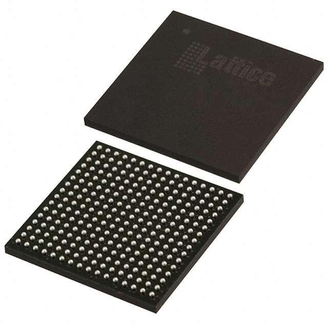
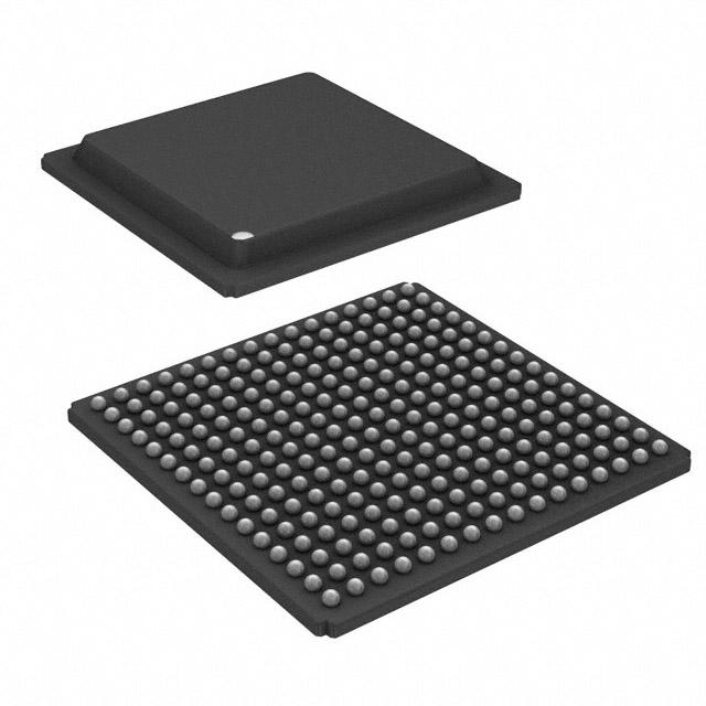
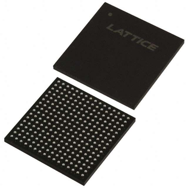
LC4256C-3FTN256BC
LC4256C-3FTN256BC ECAD Model
LC4256C-3FTN256BC Attributes
| Type | Description | Select |
|---|---|---|
| Mfr | Lattice Semiconductor Corporation | |
| Series | ispMACH® 4000C | |
| Package | Tray | |
| Programmable Type | In System Programmable | |
| Delay Time tpd(1) Max | 3 ns | |
| Voltage Supply - Internal | 1.65V ~ 1.95V | |
| Number of Logic Elements/Blocks | 16 | |
| Number of Macrocells | 256 | |
| Number of I/O | 160 | |
| Operating Temperature | 0°C ~ 90°C (TJ) | |
| Mounting Type | Surface Mount | |
| Package / Case | 256-LBGA | |
| Supplier Device Package | 256-FTBGA (17x17) | |
| Base Product Number | LC4256 |
LC4256C-3FTN256BC Datasheet Download
LC4256C-3FTN256BC Overview
The LC4256C-3FTN256BC is a Field Programmable Gate Array (FPGA) chip model manufactured by Lattice Semiconductor. It is a low-power, high-performance device with a wide range of applications.
The LC4256C-3FTN256BC has a total of 256 I/O (Input/Output) pins, and is designed for use in high-speed applications. It is also compatible with various logic families, including LVTTL, LVCMOS, and PCI. It has a maximum clock frequency of 250 MHz, and can be used for a variety of tasks such as digital signal processing, embedded system design, and image processing.
The LC4256C-3FTN256BC is also equipped with a variety of features, such as advanced I/O protection, programmable pull-up and pull-down resistors, and programmable slew rate control. In addition, it is capable of supporting up to 8 banks of DDR3/DDR2/DDR1 memory.
The LC4256C-3FTN256BC is suitable for a wide range of applications, including consumer electronics, automotive, industrial, and medical. It is also ideal for use in applications that require low power consumption, high performance, and a wide range of I/O options.
Overall, the LC4256C-3FTN256BC is a powerful, low-power FPGA chip model with a wide range of applications. It is capable of supporting up to 8 banks of DDR3/DDR2/DDR1 memory, and features advanced I/O protection, programmable pull-up and pull-down resistors, and programmable slew rate control. It is suitable for a variety of applications, including consumer electronics, automotive, industrial, and medical.
You May Also Be Interested In
4,793 In Stock
Pricing (USD)
| QTY | Unit Price | Ext Price |
|---|---|---|
| No reference price found. | ||