
Lattice Semiconductor Corporation
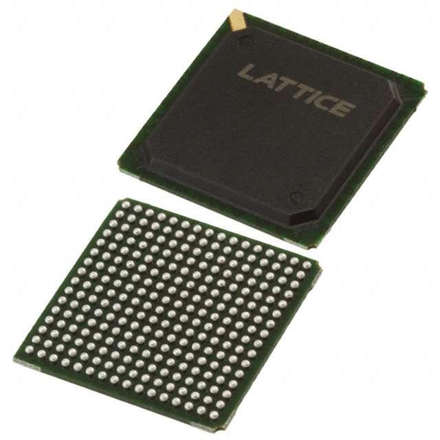
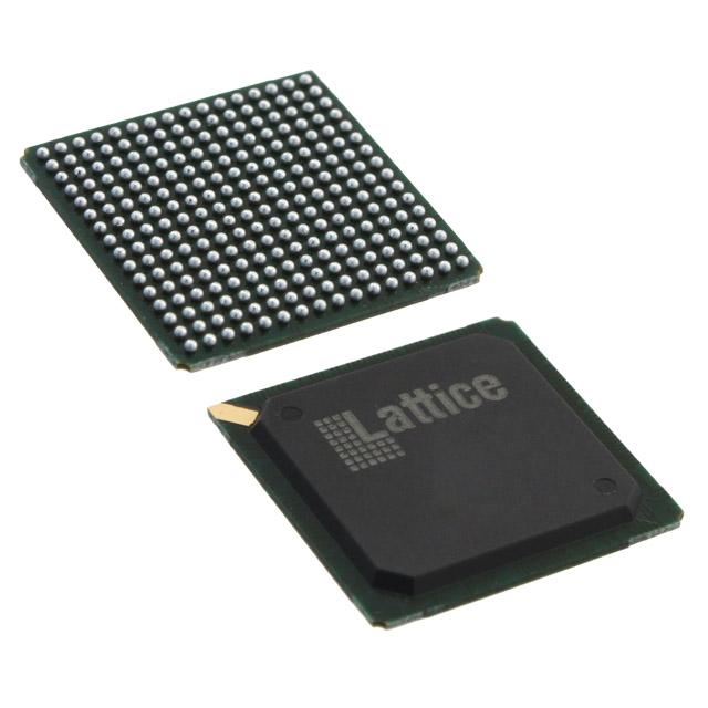
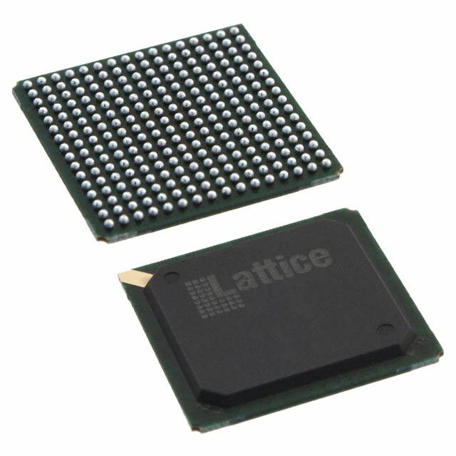
LC4256B-75FN256BC
LC4256B-75FN256BC ECAD Model
LC4256B-75FN256BC Attributes
| Type | Description | Select |
|---|---|---|
| Mfr | Lattice Semiconductor Corporation | |
| Series | ispMACH® 4000B | |
| Package | Tray | |
| Programmable Type | In System Programmable | |
| Delay Time tpd(1) Max | 7.5 ns | |
| Voltage Supply - Internal | 2.3V ~ 2.7V | |
| Number of Logic Elements/Blocks | 16 | |
| Number of Macrocells | 256 | |
| Number of I/O | 160 | |
| Operating Temperature | 0°C ~ 90°C (TJ) | |
| Mounting Type | Surface Mount | |
| Package / Case | 256-BGA | |
| Supplier Device Package | 256-FPBGA (17x17) | |
| Base Product Number | LC4256 |
LC4256B-75FN256BC Datasheet Download
LC4256B-75FN256BC Overview
The LC4256B-75FN256BC is a low-cost, high-performance Field Programmable Gate Array (FPGA) designed by Lattice Semiconductor Corporation. It is a member of the LatticeECP2/M family of FPGAs and is suitable for a wide range of applications.
The LC4256B-75FN256BC features a total of 256 logic cells, each of which contains four 6-input look-up tables (LUTs), four flip-flops, and two dedicated I/O pins. It also provides 4,096 bits of block RAM, with each block containing four RAM blocks and four DSP slices. Additionally, the device includes 16 dedicated DSP slices, providing up to 16-bit arithmetic operations, as well as four dedicated clock management tiles, with each tile providing up to four phase-locked loops (PLLs).
The LC4256B-75FN256BC is ideal for a variety of applications, including industrial control, automotive, consumer, and medical. It is designed to provide high performance and low power consumption, while still being cost-effective. It is also designed to be highly configurable, allowing developers to quickly and easily adapt the device to their specific application requirements.
In summary, the LC4256B-75FN256BC is a high-performance, low-cost FPGA designed to be suitable for a wide range of applications. It features 256 logic cells, 4,096 bits of block RAM, and 16 dedicated DSP slices, as well as four dedicated clock management tiles. Its low power consumption and configurability make it an ideal choice for a variety of applications.
You May Also Be Interested In
1,593 In Stock
Pricing (USD)
| QTY | Unit Price | Ext Price |
|---|---|---|
| No reference price found. | ||