
Lattice Semiconductor Corporation
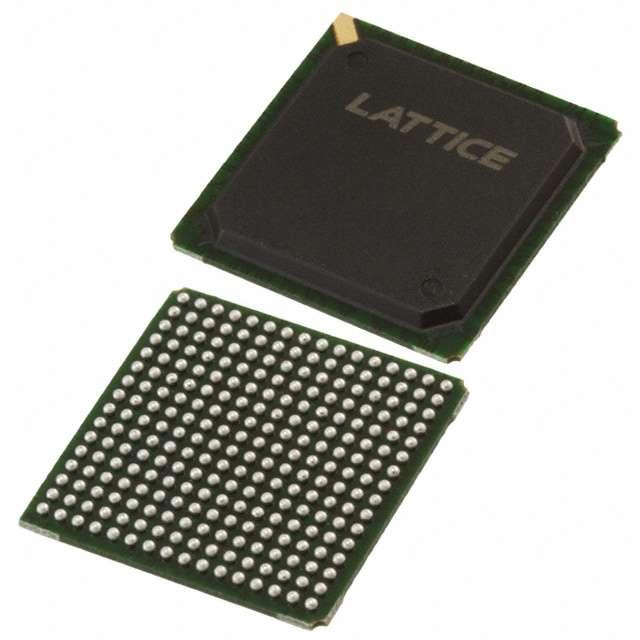
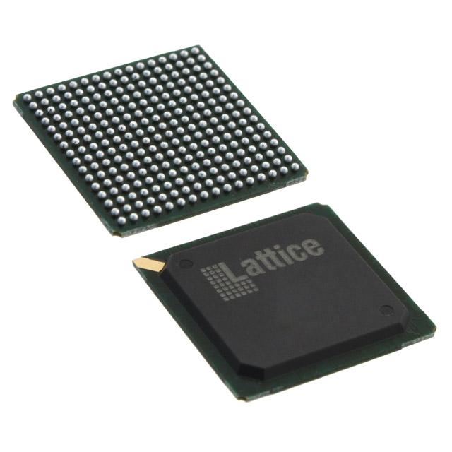
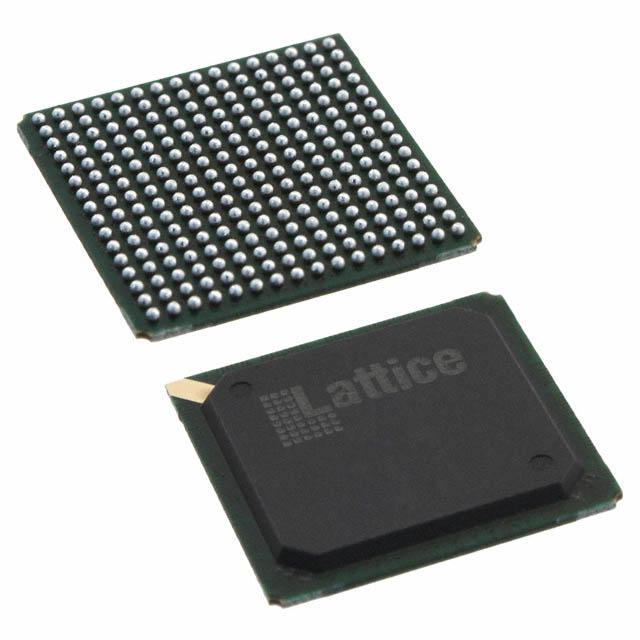
LC4256B-5FN256BI
LC4256B-5FN256BI ECAD Model
LC4256B-5FN256BI Attributes
| Type | Description | Select |
|---|---|---|
| Mfr | Lattice Semiconductor Corporation | |
| Series | ispMACH® 4000B | |
| Package | Tray | |
| Programmable Type | In System Programmable | |
| Delay Time tpd(1) Max | 5 ns | |
| Voltage Supply - Internal | 2.3V ~ 2.7V | |
| Number of Logic Elements/Blocks | 16 | |
| Number of Macrocells | 256 | |
| Number of I/O | 160 | |
| Operating Temperature | -40°C ~ 105°C (TJ) | |
| Mounting Type | Surface Mount | |
| Package / Case | 256-BGA | |
| Supplier Device Package | 256-FPBGA (17x17) | |
| Base Product Number | LC4256 |
LC4256B-5FN256BI Datasheet Download
LC4256B-5FN256BI Overview
The LC4256B-5FN256BI is a Field Programmable Gate Array (FPGA) chip manufactured by Lattice Semiconductor. It is a low-cost, low-power, high-performance, and highly configurable device.
This chip is based on a non-volatile, low-power, and high-density architecture. It features 256 macrocells, up to 4,096 Kbits of embedded RAM, and up to 4,096 Kbits of embedded ROM. It also has a total of 5,120 logic elements, and up to 4,096 Kbits of embedded Flash memory. The chip also has a wide range of I/O features, including two high-speed serial transceivers, two high-speed differential I/O banks, and two dedicated LVDS I/O banks.
The LC4256B-5FN256BI is suitable for a wide range of applications, including industrial automation, consumer electronics, automotive, medical, and military. It can be used to implement complex logic functions, and can be used to create custom logic designs. It can also be used to create custom IP cores, such as microcontrollers, processors, and memories.
The LC4256B-5FN256BI is a highly configurable device, and can be programmed using a variety of programming languages, such as Verilog, VHDL, and SystemVerilog. It is also compatible with a wide range of development tools, such as the Lattice Diamond Design Suite, the Lattice Diamond Programmer, and the Lattice Libero Integrated Design Environment (IDE).
Overall, the LC4256B-5FN256BI is a low-cost, low-power, high-performance, and highly configurable FPGA chip that can be used for a wide range of applications.
You May Also Be Interested In
4,728 In Stock
Pricing (USD)
| QTY | Unit Price | Ext Price |
|---|---|---|
| No reference price found. | ||