
Lattice Semiconductor Corporation
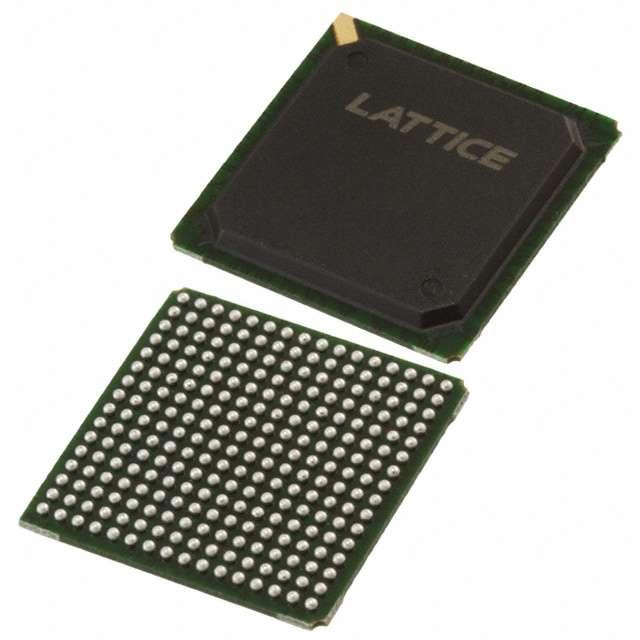
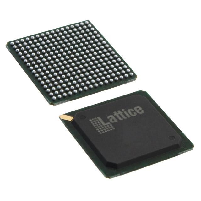
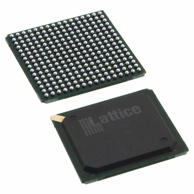
ISPLSI 5384VE-125LF256I
ISPLSI 5384VE-125LF256I ECAD Model
ISPLSI 5384VE-125LF256I Attributes
| Type | Description | Select |
|---|---|---|
| Mfr | Lattice Semiconductor Corporation | |
| Series | ispLSI® 5000VE | |
| Package | Tray | |
| Programmable Type | In System Programmable | |
| Delay Time tpd(1) Max | 7.5 ns | |
| Voltage Supply - Internal | 3V ~ 3.6V | |
| Number of Logic Elements/Blocks | 12 | |
| Number of Macrocells | 384 | |
| Number of Gates | 18000 | |
| Number of I/O | 192 | |
| Operating Temperature | -40°C ~ 85°C (TA) | |
| Mounting Type | Surface Mount | |
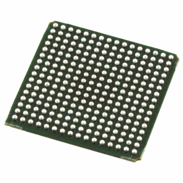
| Package / Case | 256-BGA | |
| Supplier Device Package | 256-FPBGA (17x17) | |
| Base Product Number | ISPLSI 5384VE |
ISPLSI 5384VE-125LF256I Datasheet Download
ISPLSI 5384VE-125LF256I Overview
The ISPLSI 5384VE-125LF256I is a low-power, high-performance Field Programmable Gate Array (FPGA) chip manufactured by Lattice Semiconductor. It is designed for a variety of applications, including embedded systems, communications, networking, imaging, and industrial control.
The ISPLSI 5384VE-125LF256I has an internal architecture that consists of an array of 4,096 logic cells, each containing four registers and one 4-input lookup table. It also has 16 dedicated I/O blocks, which are used to connect to external devices. The chip is capable of running at speeds of up to 125MHz and has a maximum I/O speed of 66MHz. It is also equipped with a variety of features, such as a programmable clock generator, a phase-locked loop, and a dedicated phase-locked loop output.
The ISPLSI 5384VE-125LF256I is designed to be used in a wide range of applications, including embedded systems, communications, networking, imaging, and industrial control. It is capable of supporting a variety of protocols, such as Ethernet, USB, CAN, and SPI. It also has built-in support for a variety of memory types, including Flash, SRAM, and DRAM.
In terms of power consumption, the ISPLSI 5384VE-125LF256I is designed to be highly efficient. It has an active power consumption of just 0.5W, which is significantly lower than many competing FPGA chips. It also has a standby power consumption of just 0.1W, making it an ideal choice for applications that require low power consumption.
Overall, the ISPLSI 5384VE-125LF256I is a high-performance, low-power FPGA chip that is designed for a variety of applications. It has an internal architecture that is optimized for speed and efficiency, and it is capable of supporting a wide range of protocols and memory types. It is also highly efficient in terms of power consumption, making it an ideal choice for applications that require low power consumption.
You May Also Be Interested In
4,162 In Stock
Pricing (USD)
| QTY | Unit Price | Ext Price |
|---|---|---|
| No reference price found. | ||