
Lattice Semiconductor Corporation
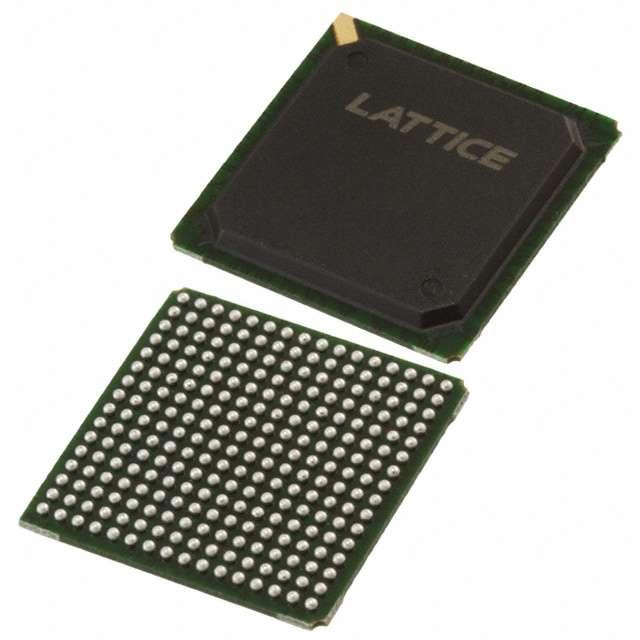
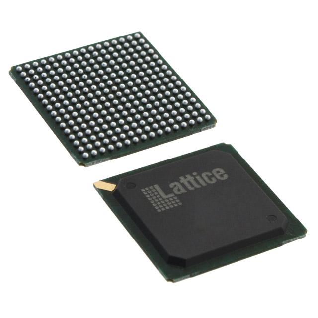
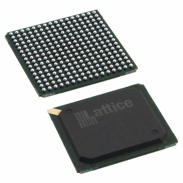
ISPLSI 5384VE-125LF256
ISPLSI 5384VE-125LF256 ECAD Model
ISPLSI 5384VE-125LF256 Attributes
| Type | Description | Select |
|---|---|---|
| Mfr | Lattice Semiconductor Corporation | |
| Series | ispLSI® 5000VE | |
| Package | Tray | |
| Programmable Type | In System Programmable | |
| Delay Time tpd(1) Max | 7.5 ns | |
| Voltage Supply - Internal | 3V ~ 3.6V | |
| Number of Logic Elements/Blocks | 12 | |
| Number of Macrocells | 384 | |
| Number of Gates | 18000 | |
| Number of I/O | 192 | |
| Operating Temperature | 0°C ~ 70°C (TA) | |
| Mounting Type | Surface Mount | |
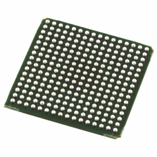
| Package / Case | 256-BGA | |
| Supplier Device Package | 256-FPBGA (17x17) | |
| Base Product Number | ISPLSI 5384VE |
ISPLSI 5384VE-125LF256 Datasheet Download
ISPLSI 5384VE-125LF256 Overview
The ISPLSI 5384VE-125LF256 is a Field Programmable Gate Array (FPGA) chip manufactured by Lattice Semiconductor Corporation. It is a low-cost, high-performance device that is ideal for use in a wide range of applications. The device has 256 macrocells, each containing 16 flip-flops and four 4-input function blocks. It also has four dedicated I/O blocks, each with 16 I/O pins, and a phase-locked loop (PLL) for clock synchronization. The device has a total of 5,120 logic elements, including 4,096 flip-flops and 1,024 four-input look-up tables (LUTs).
The device is designed to operate at a maximum frequency of 150 MHz and can be programmed using the Lattice Diamond software. It is capable of supporting a wide range of communication protocols, such as Ethernet, USB, and CANbus. It also has built-in support for a range of peripherals, such as timers, counters, and pulse-width modulation (PWM) controllers. The device can also be used in applications such as image processing, digital signal processing (DSP), and motor control.
In terms of power consumption, the device has a maximum power consumption rating of 1.5W at room temperature. The device is also compliant with the RoHS directive, making it suitable for use in a variety of applications.
Overall, the ISPLSI 5384VE-125LF256 is an excellent choice for a wide range of applications. It is a low-cost, high-performance FPGA chip that is capable of supporting a variety of communication protocols and peripherals. It is also RoHS compliant and has a low power consumption rating.
You May Also Be Interested In
5,718 In Stock
Pricing (USD)
| QTY | Unit Price | Ext Price |
|---|---|---|
| No reference price found. | ||