
Lattice Semiconductor Corporation
ISPLSI 5256VE-100LT100
ISPLSI 5256VE-100LT100 ECAD Model
ISPLSI 5256VE-100LT100 Attributes
| Type | Description | Select |
|---|---|---|
| Mfr | Lattice Semiconductor Corporation | |
| Series | ispLSI® 5000VE | |
| Package | Tray | |
| Programmable Type | In System Programmable | |
| Delay Time tpd(1) Max | 10 ns | |
| Voltage Supply - Internal | 3V ~ 3.6V | |
| Number of Logic Elements/Blocks | 8 | |
| Number of Macrocells | 256 | |
| Number of Gates | 12000 | |
| Number of I/O | 72 | |
| Operating Temperature | 0°C ~ 70°C (TA) | |
| Mounting Type | Surface Mount | |
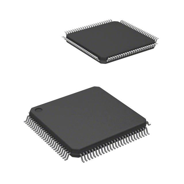
| Package / Case | 100-LQFP | |
| Supplier Device Package | 100-TQFP (14x14) | |
| Base Product Number | ISPLSI 5256VE |
ISPLSI 5256VE-100LT100 Datasheet Download
ISPLSI 5256VE-100LT100 Overview
The ISPLSI 5256VE-100LT100 is a field programmable gate array (FPGA) from Lattice Semiconductor Corporation. This chip is designed for low-cost, low-power applications and is suitable for a wide range of applications.
The ISPLSI 5256VE-100LT100 is a low-cost, low-power FPGA with a power consumption of only 100 mW. It features a 4K-bit embedded SRAM, which is ideal for applications requiring high speed and low latency. The chip has 256 logic cells and a total of 4,096 bits of embedded SRAM. It also has two dedicated clock management blocks, allowing for up to four clock signals to be generated and controlled.
The ISPLSI 5256VE-100LT100 is suitable for a wide range of applications, including industrial automation, medical, consumer, and automotive. It is also suitable for applications such as motor control, digital signal processing, and embedded system design.
The chip offers a number of features designed to make it easier to use, including a single-ended I/O interface, a rich set of I/O functions, and a wide range of user-programmable functions. Furthermore, the chip has a built-in power-on reset and a watchdog timer.
In summary, the ISPLSI 5256VE-100LT100 is a low-cost, low-power FPGA with a power consumption of only 100 mW. It is suitable for a wide range of applications and features a 4K-bit embedded SRAM, two dedicated clock management blocks, and a number of user-programmable functions.
You May Also Be Interested In

4,609 In Stock
Pricing (USD)
| QTY | Unit Price | Ext Price |
|---|---|---|
| No reference price found. | ||