

Lattice Semiconductor Corporation
ISPLSI 2096VE-250LTN128
ISPLSI 2096VE-250LTN128 ECAD Model
ISPLSI 2096VE-250LTN128 Attributes
| Type | Description | Select |
|---|---|---|
| Mfr | Lattice Semiconductor Corporation | |
| Series | ispLSI® 2000VE | |
| Package | Tray | |
| Programmable Type | In System Programmable | |
| Delay Time tpd(1) Max | 4 ns | |
| Voltage Supply - Internal | 3V ~ 3.6V | |
| Number of Logic Elements/Blocks | 24 | |
| Number of Macrocells | 96 | |
| Number of Gates | 4000 | |
| Number of I/O | 96 | |
| Operating Temperature | 0°C ~ 70°C (TA) | |
| Mounting Type | Surface Mount | |
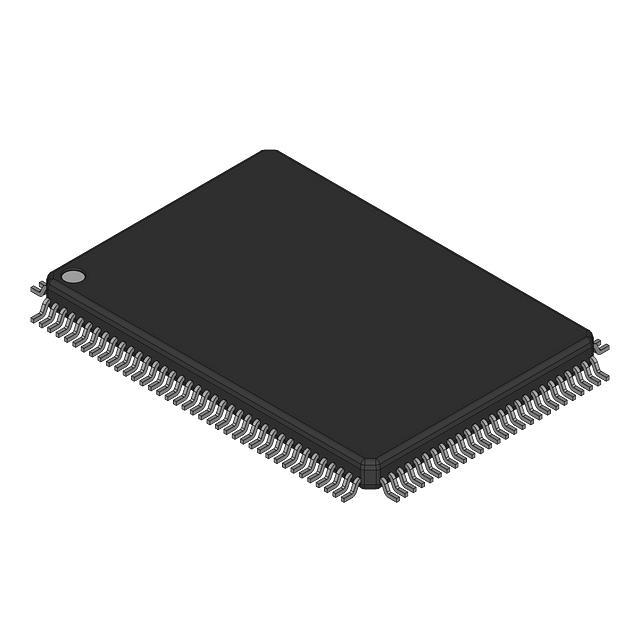
| Package / Case | 128-LQFP | |
| Supplier Device Package | 128-TQFP (14x14) | |
| Base Product Number | ISPLSI 2096VE |
ISPLSI 2096VE-250LTN128 Datasheet Download
ISPLSI 2096VE-250LTN128 Overview
The ISPLSI 2096VE-250LTN128 is a high-performance Field Programmable Gate Array (FPGA) chip model designed by Lattice Semiconductor Corporation. This model is based on the LatticeECP2M architecture, which is a low-power, highly-scalable FPGA platform. It is ideal for a wide range of applications, including embedded system design, high-end industrial control, automotive, medical, and communications.
This chip model features a total of 250K logic elements, 4.8 million system gates, and up to 1,280 user I/Os. It has an operating frequency of up to 400MHz and a maximum power dissipation of 10W. This model supports a wide range of programming languages, including Verilog, VHDL, and SystemVerilog. It also supports a variety of design tools, such as Lattice Diamond, Synplify Pro, and HDL Designer Series.
The ISPLSI 2096VE-250LTN128 has a wide range of features, including high speed, low power consumption, and scalability. It also supports a variety of memory technologies, including SRAM, DDR3, and QDR2. Additionally, this chip model is compliant with a wide range of industry standards, including JEDEC and RoHS.
In conclusion, the ISPLSI 2096VE-250LTN128 is a powerful and versatile FPGA chip model designed by Lattice Semiconductor Corporation. This model is ideal for a wide range of applications, including embedded system design, high-end industrial control, automotive, medical, and communications. It features high speed, low power consumption, and scalability. Additionally, it supports a variety of memory technologies and is compliant with a wide range of industry standards.
You May Also Be Interested In
5,595 In Stock
Pricing (USD)
| QTY | Unit Price | Ext Price |
|---|---|---|
| No reference price found. | ||