

Lattice Semiconductor Corporation
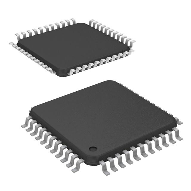
ISPLSI 2064VE-100LT44
ISPLSI 2064VE-100LT44 ECAD Model
ISPLSI 2064VE-100LT44 Attributes
| Type | Description | Select |
|---|---|---|
| Mfr | Lattice Semiconductor Corporation | |
| Series | ispLSI® 2000VE | |
| Package | Box | |
| Programmable Type | In System Programmable | |
| Delay Time tpd(1) Max | 10 ns | |
| Voltage Supply - Internal | 3V ~ 3.6V | |
| Number of Logic Elements/Blocks | 16 | |
| Number of Macrocells | 64 | |
| Number of Gates | 2000 | |
| Number of I/O | 32 | |
| Operating Temperature | 0°C ~ 70°C (TA) | |
| Mounting Type | Surface Mount | |
| Package / Case | 44-TQFP | |
| Supplier Device Package | 44-TQFP (10x10) | |
| Base Product Number | ISPLSI 2064VE |
ISPLSI 2064VE-100LT44 Datasheet Download
ISPLSI 2064VE-100LT44 Overview
The ISPLSI 2064VE-100LT44 is an advanced FPGA (Field Programmable Gate Array) chip from Lattice Semiconductor Corporation. It is a high-performance, low-cost, low-power device designed for a wide range of applications.
The ISPLSI 2064VE-100LT44 is a 4-input, 4-output (4-I/O) device with a maximum operating frequency of 100 MHz. It has a total of 4,096 logic elements (LEs), each of which is capable of implementing up to 4-input logic functions. It also features a total of 1,024 flip-flops and 2,048 RAM bits. The device is fabricated using a 0.25-micron CMOS process.
The ISPLSI 2064VE-100LT44 is suitable for a wide range of applications, including digital signal processing, data acquisition, image processing, communications, and embedded systems. It is also suitable for applications requiring a low-cost, low-power solution. The device is compliant with the IEEE 1149.1 JTAG boundary scan standard, allowing for easy debugging and testing.
In summary, the ISPLSI 2064VE-100LT44 is a high-performance, low-cost, low-power FPGA device from Lattice Semiconductor Corporation. It is suitable for a wide range of applications, including digital signal processing, data acquisition, image processing, communications, and embedded systems. It features a total of 4,096 LEs, 1,024 flip-flops and 2,048 RAM bits, and is compliant with the IEEE 1149.1 JTAG boundary scan standard.
You May Also Be Interested In


3,101 In Stock
Pricing (USD)
| QTY | Unit Price | Ext Price |
|---|---|---|
| No reference price found. | ||