
Intel Corporation
5SGXMA7N2F40I3N
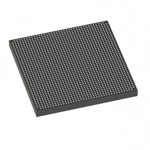
5SGXMA7N2F40I3N ECAD Model
5SGXMA7N2F40I3N Attributes
| Type | Description | Select |
|---|---|---|
| Mfr | Intel | |
| Series | Stratix® V GX | |
| Package | Tray | |
| Number of LABs/CLBs | 234720 | |
| Number of Logic Elements/Cells | 622000 | |
| Total RAM Bits | 51200000 | |
| Number of I/O | 600 | |
| Voltage - Supply | 0.82V ~ 0.88V | |
| Mounting Type | Surface Mount | |
| Operating Temperature | -40°C ~ 100°C (TJ) | |
| Package / Case | 1517-BBGA, FCBGA | |
| Supplier Device Package | 1517-FBGA (40x40) | |
| Base Product Number | 5SGXMA7 |
5SGXMA7N2F40I3N Datasheet Download
5SGXMA7N2F40I3N Overview
The 5SGXMA7N2F40I3N is an Altera Stratix V FPGA chip model. It is an advanced FPGA that includes a high-performance, high-density logic fabric, hardened transceivers, and a variety of embedded memory blocks. This chip has a total of 1,944,000 logic elements, 36,864 Kbits of embedded memory and 1,536 18x18 multipliers. It also has 5,184 I/O pins, which can be configured as LVDS, LVPECL, or SSTL.
The 5SGXMA7N2F40I3N is ideal for applications requiring high-speed processing, such as high-end networking, telecommunications, and video processing. It is also suitable for applications that require high-density memory and logic, such as embedded systems and ASIC prototyping.
The 5SGXMA7N2F40I3N is a high-performance FPGA that offers a number of advantages over traditional ASICs. It is more flexible and can be quickly reconfigured for different applications. It is also more cost-effective, since it can be used in a variety of applications without the need for costly redesigns.
The 5SGXMA7N2F40I3N is a powerful and versatile FPGA that can be used in a variety of applications. It is ideal for applications requiring high-speed processing, high-density memory and logic, and flexibility. It is also cost-effective, since it can be quickly reconfigured without expensive redesigns.
You May Also Be Interested In

1,951 In Stock
Pricing (USD)
| QTY | Unit Price | Ext Price |
|---|---|---|
| No reference price found. | ||