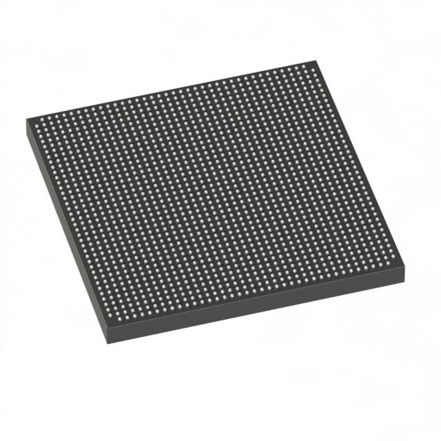
Intel Corporation
5SGXMA7N2F40C2LN
5SGXMA7N2F40C2LN ECAD Model
5SGXMA7N2F40C2LN Attributes
| Type | Description | Select |
|---|---|---|
| Mfr | Intel | |
| Series | Stratix® V GX | |
| Package | Tray | |
| Number of LABs/CLBs | 234720 | |
| Number of Logic Elements/Cells | 622000 | |
| Total RAM Bits | 51200000 | |
| Number of I/O | 600 | |
| Voltage - Supply | 0.82V ~ 0.88V | |
| Mounting Type | Surface Mount | |
| Operating Temperature | 0°C ~ 85°C (TJ) | |
| Package / Case | 1517-BBGA, FCBGA | |
| Supplier Device Package | 1517-FBGA (40x40) | |
| Base Product Number | 5SGXMA7 |
5SGXMA7N2F40C2LN Datasheet Download
5SGXMA7N2F40C2LN Overview
The 5SGXMA7N2F40C2LN chip model is an FPGA (Field Programmable Gate Array) from Intel's Stratix 10 family. It is designed to provide high performance and flexibility for a wide range of applications. The chip features a large number of logic elements, memory blocks, and transceivers, as well as a wide range of I/O options.
The 5SGXMA7N2F40C2LN chip has a total of 3.9 million logic elements and over 4,000 memory blocks. It also includes 4,096 I/O pins and up to 128 transceivers. It has a maximum clock frequency of 400 MHz, and a maximum power consumption of 25 W. It is available in a package size of 11.5 x 11.5 mm.
The 5SGXMA7N2F40C2LN chip is suitable for a wide range of applications, including embedded systems, industrial automation, medical imaging, and communications. It can be used for applications that require high performance and flexibility, such as real-time image processing, machine learning, and data analytics.
The 5SGXMA7N2F40C2LN chip is designed to be highly reliable and offers a long product life. It is also designed to be easy to use and program, with a wide range of development tools available. The chip is also designed for low power consumption, making it suitable for battery-powered applications.
You May Also Be Interested In
1,627 In Stock
Pricing (USD)
| QTY | Unit Price | Ext Price |
|---|---|---|
| No reference price found. | ||

