
Intel Corporation
5SGXMA7K1F35C2N
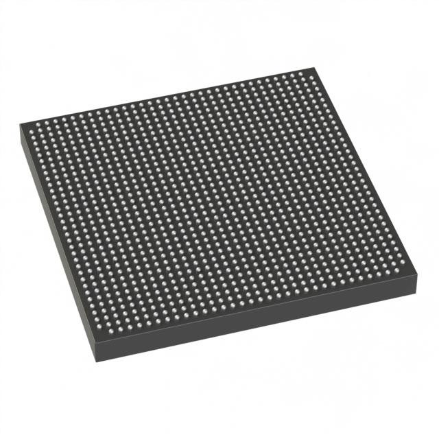
5SGXMA7K1F35C2N ECAD Model
5SGXMA7K1F35C2N Attributes
| Type | Description | Select |
|---|---|---|
| Mfr | Intel | |
| Series | Stratix® V GX | |
| Package | Tray | |
| Number of LABs/CLBs | 234720 | |
| Number of Logic Elements/Cells | 622000 | |
| Total RAM Bits | 51200000 | |
| Number of I/O | 432 | |
| Voltage - Supply | 0.87V ~ 0.93V | |
| Mounting Type | Surface Mount | |
| Operating Temperature | 0°C ~ 85°C (TJ) | |
| Package / Case | 1152-BBGA, FCBGA | |
| Supplier Device Package | 1152-FBGA (35x35) | |
| Base Product Number | 5SGXMA7 |
5SGXMA7K1F35C2N Datasheet Download
5SGXMA7K1F35C2N Overview
The 5SGXMA7K1F35C2N is an Altera Stratix V FPGA, part of the Stratix V family of FPGAs. It is a high-end device, designed for applications that require high-performance and low-power consumption.
The FPGA features an advanced transceiver technology, which allows for high-speed data transfer. It has a total of 1,152,000 logic elements, including 5,120 embedded memory blocks and up to 1,920 18x18 multipliers. It also has up to 1,152 DSP blocks, and up to 5,120 I/O pins. The device is available in a variety of packages, including a 672-ball BGA and a 676-pin FBGA.
The 5SGXMA7K1F35C2N is suitable for a wide range of applications, such as high-end networking, embedded systems, and military/aerospace applications. It can be used for applications such as video and image processing, high-speed serial communication, and high-speed signal processing.
The FPGA is designed to meet the needs of demanding applications, and it is capable of delivering high-performance, low-power, and reliable operation. It is also designed to be compatible with a wide range of development tools, allowing for rapid prototyping and debugging.
You May Also Be Interested In

3,466 In Stock
Pricing (USD)
| QTY | Unit Price | Ext Price |
|---|---|---|
| No reference price found. | ||