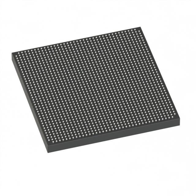
Intel Corporation
5SGXEB6R2F40I3N
5SGXEB6R2F40I3N ECAD Model
5SGXEB6R2F40I3N Attributes
| Type | Description | Select |
|---|---|---|
| Rohs Code | Yes | |
| Part Life Cycle Code | Obsolete | |
| Supply Voltage-Nom | 850 mV | |
| Number of Inputs | 432 | |
| Number of Outputs | 432 | |
| Number of Logic Cells | 597000 | |
| Number of CLBs | 22540 | |
| Programmable Logic Type | FIELD PROGRAMMABLE GATE ARRAY | |
| Temperature Grade | INDUSTRIAL | |
| Package Shape | SQUARE | |
| Technology | CMOS | |
| Organization | 22540 CLBS | |
| Power Supplies | 0.85,1.5,2.5,2.5/3,1.2/3 V | |
| Supply Voltage-Max | 880 mV | |
| Supply Voltage-Min | 820 mV | |
| JESD-30 Code | S-PBGA-B1517 | |
| Qualification Status | Not Qualified | |
| Operating Temperature-Max | 100 °C | |
| Operating Temperature-Min | -40 °C | |
| Peak Reflow Temperature (Cel) | NOT SPECIFIED | |
| Time@Peak Reflow Temperature-Max (s) | NOT SPECIFIED | |
| Number of Terminals | 1517 | |
| Package Body Material | PLASTIC/EPOXY | |
| Package Code | BGA | |
| Package Equivalence Code | BGA1517,39X39,40 | |
| Package Shape | SQUARE | |
| Package Style | GRID ARRAY | |
| Surface Mount | YES | |
| Terminal Form | BALL | |
| Terminal Pitch | 1 mm | |
| Terminal Position | BOTTOM | |
| Width | 40 mm | |
| Length | 40 mm | |
| Seated Height-Max | 3.5 mm | |
| Ihs Manufacturer | INTEL CORP | |
| Package Description | FBGA-1517 | |
| Reach Compliance Code | compliant | |
| ECCN Code | 3A001.A.7.B | |
| HTS Code | 8542.39.00.01 |
5SGXEB6R2F40I3N Datasheet Download
5SGXEB6R2F40I3N Overview
The chip model 5SGXEB6R2F40I3N is a highly advanced integrated circuit from Altera, a leading semiconductor manufacturer. It is a powerful and versatile solution for a wide range of applications, including high-performance digital signal processing, embedded processing, image processing, and more.
The 5SGXEB6R2F40I3N is built on a 40nm CMOS process and features a high-performance FPGA fabric with a wide range of features, including up to 8,192 logic elements, up to 4,096Kbits of embedded SRAM, up to 8,192Kbits of embedded ROM, up to 192Kbits of embedded RAM, and up to 8,192Kbits of embedded ROM. It also supports up to 32 transceivers with data rates of up to 12.5Gbps. This makes it an ideal choice for a variety of applications.
The 5SGXEB6R2F40I3N is programmed using a hardware description language (HDL) such as VHDL or Verilog. This allows designers to create complex systems that can be quickly and easily implemented on the chip. Additionally, the chip offers a wide range of features, such as on-chip debugging, an integrated JTAG interface, and an integrated DSP block.
The 5SGXEB6R2F40I3N offers a number of advantages over other solutions. It has a low power consumption and a high level of integration, which makes it ideal for embedded and mobile applications. Additionally, it is a highly scalable solution, allowing designers to easily configure the chip for different applications. Finally, it is a cost-effective solution, offering a low total cost of ownership.
The demand for the 5SGXEB6R2F40I3N is expected to increase in the coming years, as more and more applications require high-performance, low-power solutions. This chip is well-suited for a wide range of applications, such as digital signal processing, embedded processing, image processing, and more. Additionally, the chip is highly configurable, allowing designers to tailor it to their specific needs.
When designing with the 5SGXEB6R2F40I3N, it is important to consider the specific requirements of the application. This includes the type of signal processing, the type of embedded processing, the type of image processing, and any other specific requirements. Additionally, designers should be aware of the power requirements of the chip, as well as the available pins and other features.
Finally, when designing with the 5SGXEB6R2F40I3N, it is important to be aware of the potential risks. These include the possibility of overloading the chip, which can cause it to malfunction or even fail. Additionally, designers should be aware of the potential for signal interference, as well as the possibility of data corruption. By taking these precautions, designers can ensure that their designs are successful.
You May Also Be Interested In
5,984 In Stock
Pricing (USD)
| QTY | Unit Price | Ext Price |
|---|---|---|
| 1+ | $8,094.7349 | $8,094.7349 |
| 10+ | $8,007.6947 | $80,076.9472 |
| 100+ | $7,572.4939 | $757,249.3920 |
| 1000+ | $7,137.2931 | $3,568,646.5600 |
| 10000+ | $6,528.0120 | $6,528,012.0000 |
| The price is for reference only, please refer to the actual quotation! | ||

