Intel Corporation
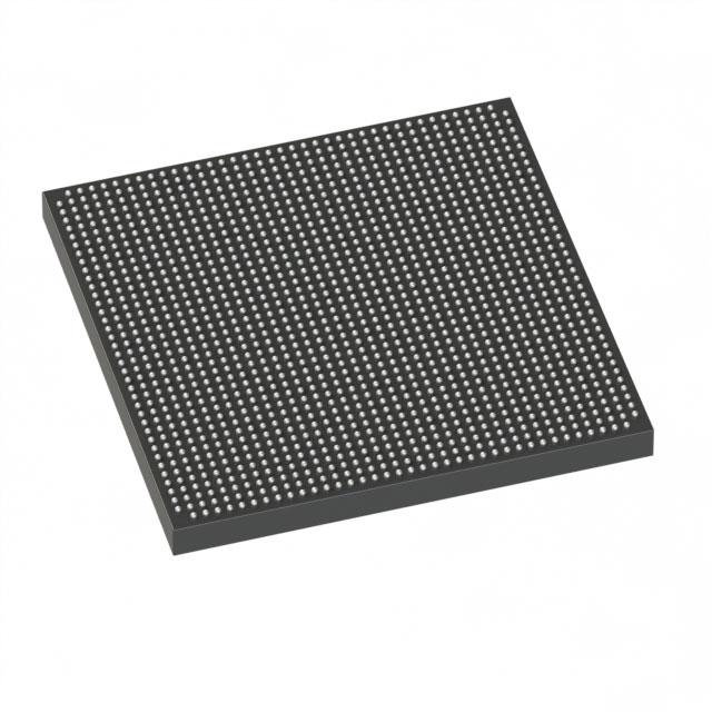
5SGXEB5R2F40I3LN
5SGXEB5R2F40I3LN ECAD Model
5SGXEB5R2F40I3LN Attributes
| Type | Description | Select |
|---|---|---|
| Mfr | Intel | |
| Series | Stratix® V GX | |
| Package | Tray | |
| Number of LABs/CLBs | 185000 | |
| Number of Logic Elements/Cells | 490000 | |
| Total RAM Bits | 41984000 | |
| Number of I/O | 432 | |
| Voltage - Supply | 0.82V ~ 0.88V | |
| Mounting Type | Surface Mount | |
| Operating Temperature | -40°C ~ 100°C (TJ) | |
| Package / Case | 1517-FBGA (40x40) | |
| Supplier Device Package | 1517-FBGA (40x40) | |
| Base Product Number | 5SGXEB5 |
5SGXEB5R2F40I3LN Datasheet Download
5SGXEB5R2F40I3LN Overview
The 5SGXEB5R2F40I3LN is an Altera FPGA chip model that belongs to the Stratix V family. It is a high-performance, low-power FPGA device that is ideal for applications that require high performance and low power consumption. It has a total of 40,320 logic elements, and a total of 1.4 million logic gates. It also has 1,920 DSP blocks and 1,920 embedded memory blocks. The chip has a total of 4,096 18x18 multipliers and a total of 4,096 72-bit RAM blocks.
The 5SGXEB5R2F40I3LN is a high-speed FPGA, with a maximum operating frequency of up to 1.2 GHz, and a maximum clock frequency of up to 1.5 GHz. It also has a total of 1,536 I/Os, with a total of 1,280 differential I/Os and 256 single-ended I/Os. It also has a total of 48 phase-locked loops and a total of 48 transceivers.
The 5SGXEB5R2F40I3LN is ideal for applications such as high-speed networking, video and image processing, embedded system design, and high-performance computing. It is also suitable for applications such as automotive, aerospace, industrial, and medical. It is also suitable for applications such as military and defense, and communications.
In conclusion, the 5SGXEB5R2F40I3LN is a high-performance, low-power FPGA chip model that is suitable for a wide range of applications. It has a total of 40,320 logic elements, 1.4 million logic gates, 1,920 DSP blocks, 1,920 embedded memory blocks, 4,096 18x18 multipliers, 4,096 72-bit RAM blocks, 48 phase-locked loops, and 48 transceivers. It is ideal for applications such as high-speed networking, video and image processing, embedded system design, and high-performance computing.
You May Also Be Interested In
5,647 In Stock
Pricing (USD)
| QTY | Unit Price | Ext Price |
|---|---|---|
| No reference price found. | ||


