
Intel Corporation
5SGXEB5R2F40C1N
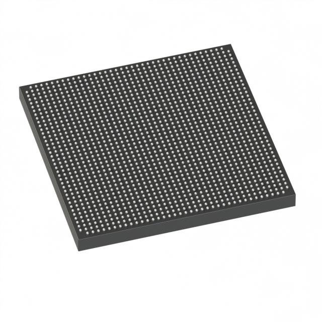
5SGXEB5R2F40C1N ECAD Model
5SGXEB5R2F40C1N Attributes
| Type | Description | Select |
|---|---|---|
| Mfr | Intel | |
| Series | Stratix® V GX | |
| Package | Tray | |
| Number of LABs/CLBs | 185000 | |
| Number of Logic Elements/Cells | 490000 | |
| Total RAM Bits | 41984000 | |
| Number of I/O | 432 | |
| Voltage - Supply | 0.87V ~ 0.93V | |
| Mounting Type | Surface Mount | |
| Operating Temperature | 0°C ~ 85°C (TJ) | |
| Package / Case | 1517-FBGA (40x40) | |
| Supplier Device Package | 1517-FBGA (40x40) | |
| Base Product Number | 5SGXEB5 |
5SGXEB5R2F40C1N Datasheet Download
5SGXEB5R2F40C1N Overview
The 5SGXEB5R2F40C1N is an Altera FPGA (Field Programmable Gate Array) chip manufactured by Intel. It is part of the Stratix V family of FPGAs and is based on the Stratix V GX architecture. It is a high-performance, low-power FPGA with a wide range of features.
The 5SGXEB5R2F40C1N has a total of 1,536,000 logic elements, including 3,450 embedded memory blocks and 6,912 18-Kb RAM blocks. It also has over 11,000 18-Kb RAM blocks and over 14,000 18-Kb ROM blocks. It has four banks of high-speed transceivers, which support up to 28 Gb/s data rates. The chip also has a wide range of I/O features, including up to 144 differential I/O pairs, up to 216 single-ended I/O pairs, and up to 72 LVDS I/O pairs.
The 5SGXEB5R2F40C1N is suitable for a wide range of applications, including high-performance embedded systems, high-speed communications, video processing, and military/aerospace applications. It is ideal for applications that require high levels of performance, low power consumption, and a wide range of features.
The 5SGXEB5R2F40C1N is an advanced, high-performance FPGA chip that offers a wide range of features and capabilities. It is suitable for a range of demanding applications, and is capable of delivering high levels of performance while consuming low levels of power.
You May Also Be Interested In


4,702 In Stock
Pricing (USD)
| QTY | Unit Price | Ext Price |
|---|---|---|
| No reference price found. | ||