
Intel Corporation
5SGXEA9K2H40I2L
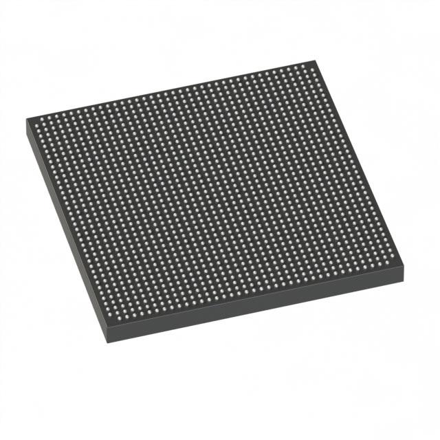
5SGXEA9K2H40I2L ECAD Model
5SGXEA9K2H40I2L Attributes
| Type | Description | Select |
|---|---|---|
| Mfr | Intel | |
| Series | Stratix® V GX | |
| Package | Tray | |
| Number of LABs/CLBs | 317000 | |
| Number of Logic Elements/Cells | 840000 | |
| Total RAM Bits | 53248000 | |
| Number of I/O | 696 | |
| Voltage - Supply | 0.82V ~ 0.88V | |
| Mounting Type | Surface Mount | |
| Operating Temperature | -40°C ~ 100°C (TJ) | |
| Package / Case | 1517-BBGA, FCBGA | |
| Supplier Device Package | 1517-HBGA (45x45) | |
| Base Product Number | 5SGXEA9 |
5SGXEA9K2H40I2L Datasheet Download
5SGXEA9K2H40I2L Overview
The 5SGXEA9K2H40I2L is an Altera Stratix V FPGA chip model. It is a high-end device that offers a combination of high performance, low power consumption, and advanced features. It is designed for a wide range of applications including embedded systems, networking, and communications.
The 5SGXEA9K2H40I2L has a total of 40,960 logic elements, 1,536 18-bit embedded multipliers, 6,144 Kbits of embedded RAM, and 1,536 18x18-bit DSP blocks. It also has four transceivers that support 10.3125 Gbps data rates. The chip has a power consumption of up to 13.5 W and operates at a temperature range of 0°C to 85°C.
The 5SGXEA9K2H40I2L supports a wide range of I/O standards including LVDS, PCI Express, Gigabit Ethernet, and SRIO. It also supports a variety of protocols such as SPI, I2C, UART, and CAN. Furthermore, it has an integrated JTAG/Boundary Scan Test (BST) interface for debugging and testing.
The 5SGXEA9K2H40I2L is suitable for a variety of applications including embedded systems, networking, and communications. It can be used for high-speed data processing, high-speed signal processing, and data acquisition. It is an ideal choice for applications that require high performance, low power consumption, and advanced features.
You May Also Be Interested In

4,134 In Stock
Pricing (USD)
| QTY | Unit Price | Ext Price |
|---|---|---|
| No reference price found. | ||