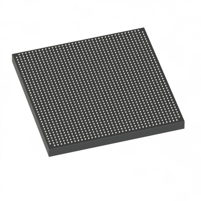
Intel Corporation
5SGXEA7K3F40C2
5SGXEA7K3F40C2 ECAD Model
5SGXEA7K3F40C2 Attributes
| Type | Description | Select |
|---|---|---|
| Mfr | Intel | |
| Series | Stratix® V GX | |
| Package | Tray | |
| Number of LABs/CLBs | 234720 | |
| Number of Logic Elements/Cells | 622000 | |
| Total RAM Bits | 51200000 | |
| Number of I/O | 696 | |
| Voltage - Supply | 0.87V ~ 0.93V | |
| Mounting Type | Surface Mount | |
| Operating Temperature | 0°C ~ 85°C (TJ) | |
| Package / Case | 1517-BBGA, FCBGA | |
| Supplier Device Package | 1517-FBGA (40x40) | |
| Base Product Number | 5SGXEA7 |
5SGXEA7K3F40C2 Datasheet Download
5SGXEA7K3F40C2 Overview
The 5SGXEA7K3F40C2 is a member of the Stratix V family of FPGAs from Intel. This model is a high-performance, low-power FPGA, designed for a variety of applications in the industrial, communications, and military sectors.
The 5SGXEA7K3F40C2 is a two-dimensional array of logic elements, each containing four input/output pins and two logic elements. The logic elements are connected to the pins via multiplexers, allowing for the implementation of complex functions. The device also has a high-speed transceiver, which supports up to 12.5 Gbps data rates.
The 5SGXEA7K3F40C2 is designed for a wide range of applications, including high-speed networking, digital signal processing, and embedded systems. It supports a variety of protocols, such as Ethernet, PCI Express, and USB. The device also features an on-chip memory controller, which supports DDR3 and DDR4 memory interfaces.
The 5SGXEA7K3F40C2 is a high-performance device, capable of providing up to 8.2 billion logic elements per second. It is also power-efficient, with a typical power consumption of only 0.9 watts. Additionally, the device is highly reliable, with a mean time between failures (MTBF) of up to 1.2 million hours.
Overall, the 5SGXEA7K3F40C2 is a high-performance, low-power FPGA, designed for a variety of applications in the industrial, communications, and military sectors. It is capable of providing up to 8.2 billion logic elements per second, while consuming only 0.9 watts of power. The device also features an on-chip memory controller, which supports DDR3 and DDR4 memory interfaces, as well as a high-speed transceiver, which supports up to 12.5 Gbps data rates.
You May Also Be Interested In
4,732 In Stock
Pricing (USD)
| QTY | Unit Price | Ext Price |
|---|---|---|
| No reference price found. | ||


