Intel Corporation
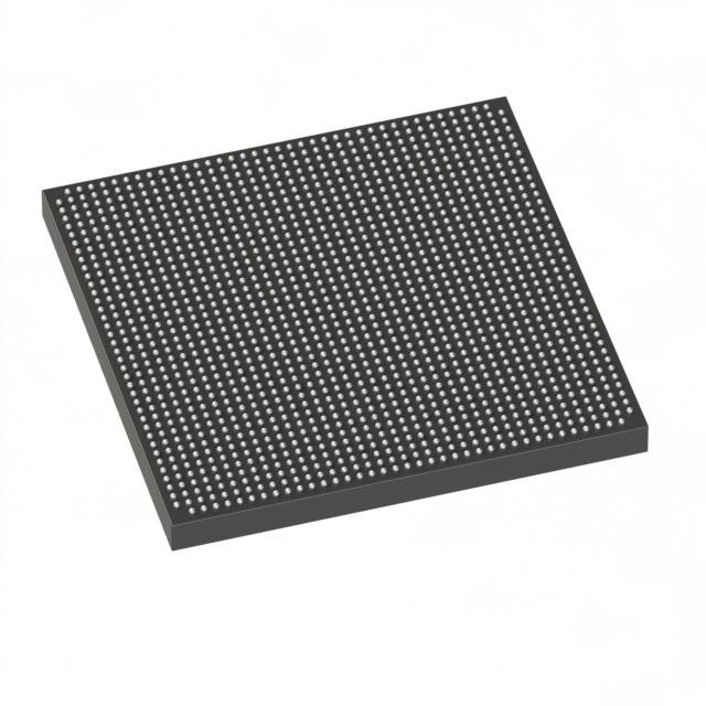
5SGXEA5N3F40C2G
5SGXEA5N3F40C2G ECAD Model
5SGXEA5N3F40C2G Attributes
| Type | Description | Select |
|---|---|---|
| Part Life Cycle Code | Active | |
| Programmable Logic Type | FIELD PROGRAMMABLE GATE ARRAY | |
| Peak Reflow Temperature (Cel) | NOT SPECIFIED | |
| Time@Peak Reflow Temperature-Max (s) | NOT SPECIFIED | |
| Ihs Manufacturer | INTEL CORP | |
| Reach Compliance Code | compliant | |
| HTS Code | 8542.39.00.01 |
5SGXEA5N3F40C2G Datasheet Download
5SGXEA5N3F40C2G Overview
The chip model 5SGXEA5N3F40C2G is a high-performance, low-power field programmable gate array (FPGA) designed to meet the needs of a wide range of applications. Its original design intention was to provide a flexible, cost-effective solution for a broad range of applications, including advanced communication systems. It is capable of supporting a wide range of communication protocols, such as Ethernet, USB, and PCI Express.
The 5SGXEA5N3F40C2G is also suitable for future upgrades. It is equipped with a wide range of features that enable it to be upgraded for improved performance and functionality. It can be used for a variety of intelligent scenarios, such as machine learning, deep learning, and natural language processing. It can also be used in the era of fully intelligent systems.
The 5SGXEA5N3F40C2G is designed to provide a high level of performance and flexibility. It has a wide range of features, including high-speed transceivers, multiple I/O banks, and a high-performance processor. It is designed to meet the needs of a wide range of applications, including those in communication systems. It is also designed to provide a cost-effective solution for a broad range of applications.
When using the 5SGXEA5N3F40C2G, it is important to consider the specific design requirements. It is important to ensure that the circuit design is optimized for the intended application to maximize performance and reduce power consumption. It is also important to consider any potential risks associated with the design, such as electromagnetic interference.
Case studies and actual implementations of the 5SGXEA5N3F40C2G can provide valuable insight into the design process. For example, a case study of a successful implementation of the 5SGXEA5N3F40C2G in a communication system can provide valuable information on how to optimize the design for the intended application.
In conclusion, the 5SGXEA5N3F40C2G is a high-performance, low-power FPGA designed to meet the needs of a wide range of applications, including advanced communication systems. It can be used for a variety of intelligent scenarios and is suitable for future upgrades. It is important to consider the specific design requirements and potential risks associated with the design when using the 5SGXEA5N3F40C2G. Case studies and actual implementations can provide valuable insight into the design process.
You May Also Be Interested In
1,840 In Stock
Pricing (USD)
| QTY | Unit Price | Ext Price |
|---|---|---|
| 1+ | $26,765.0343 | $26,765.0343 |
| 10+ | $26,477.2383 | $264,772.3826 |
| 100+ | $25,038.2579 | $2,503,825.7916 |
| 1000+ | $23,599.2776 | $11,799,638.7880 |
| 10000+ | $21,584.7051 | $21,584,705.1000 |
| The price is for reference only, please refer to the actual quotation! | ||

