
Intel Corporation
5SGXEA5H2F35I3
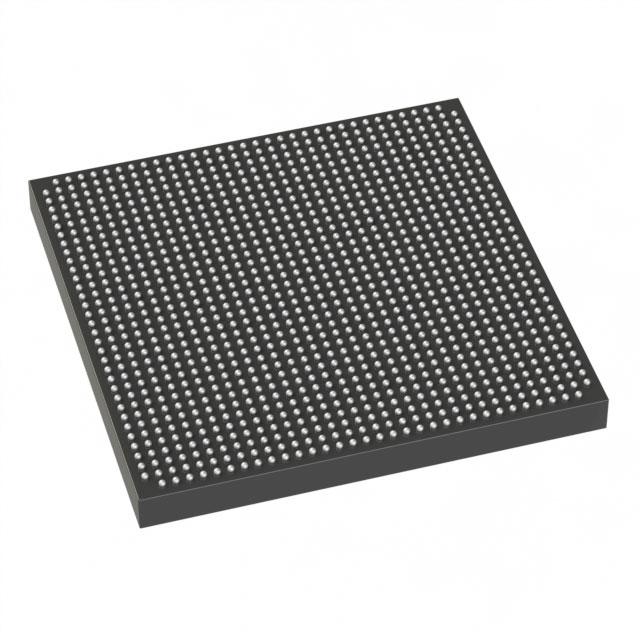
5SGXEA5H2F35I3 ECAD Model
5SGXEA5H2F35I3 Attributes
| Type | Description | Select |
|---|---|---|
| Mfr | Intel | |
| Series | Stratix® V GX | |
| Package | Tray | |
| Number of LABs/CLBs | 185000 | |
| Number of Logic Elements/Cells | 490000 | |
| Total RAM Bits | 46080000 | |
| Number of I/O | 552 | |
| Voltage - Supply | 0.82V ~ 0.88V | |
| Mounting Type | Surface Mount | |
| Operating Temperature | -40°C ~ 100°C (TJ) | |
| Package / Case | 1152-BBGA, FCBGA | |
| Supplier Device Package | 1152-FBGA (35x35) | |
| Base Product Number | 5SGXEA5 |
5SGXEA5H2F35I3 Datasheet Download
5SGXEA5H2F35I3 Overview
The 5SGXEA5H2F35I3 chip model is an FPGA (Field Programmable Gate Array) manufactured by Altera. It is a high-end device that is part of the Stratix V GX family. This model is available in a 576-pin FBGA package and is capable of operating at a maximum clock rate of 400 MHz.
The 5SGXEA5H2F35I3 chip offers a wide range of features, including up to 1.6 million logic elements, up to 1.6 million flip-flops and up to 28,672 Kbits of embedded RAM. It also offers support for up to 2,500 user-defined I/Os and up to 1,024 GXB transceivers.
This chip model is suitable for a variety of applications, such as high-speed networking, video processing, wireless communication, and embedded systems. It is also suitable for applications that require high-speed, low-power design solutions.
The 5SGXEA5H2F35I3 chip is compliant with the latest industry standards, including JTAG, IEEE 1532, and IEEE 1149.1. It is also compliant with the Open Core Protocol (OCP) and is designed to be compatible with a wide range of third-party software tools.
Overall, the 5SGXEA5H2F35I3 chip is a powerful and reliable FPGA device that is suitable for a variety of applications. It offers a wide range of features and is compliant with the latest industry standards.
You May Also Be Interested In

4,233 In Stock
Pricing (USD)
| QTY | Unit Price | Ext Price |
|---|---|---|
| No reference price found. | ||