
Intel Corporation
5SGXEA3K2F35I3LN
5SGXEA3K2F35I3LN ECAD Model
5SGXEA3K2F35I3LN Attributes
| Type | Description | Select |
|---|---|---|
| Mfr | Intel | |
| Series | Stratix® V GX | |
| Package | Tray | |
| Number of LABs/CLBs | 128300 | |
| Number of Logic Elements/Cells | 340000 | |
| Total RAM Bits | 19456000 | |
| Number of I/O | 432 | |
| Voltage - Supply | 0.82V ~ 0.88V | |
| Mounting Type | Surface Mount | |
| Operating Temperature | -40°C ~ 100°C (TJ) | |
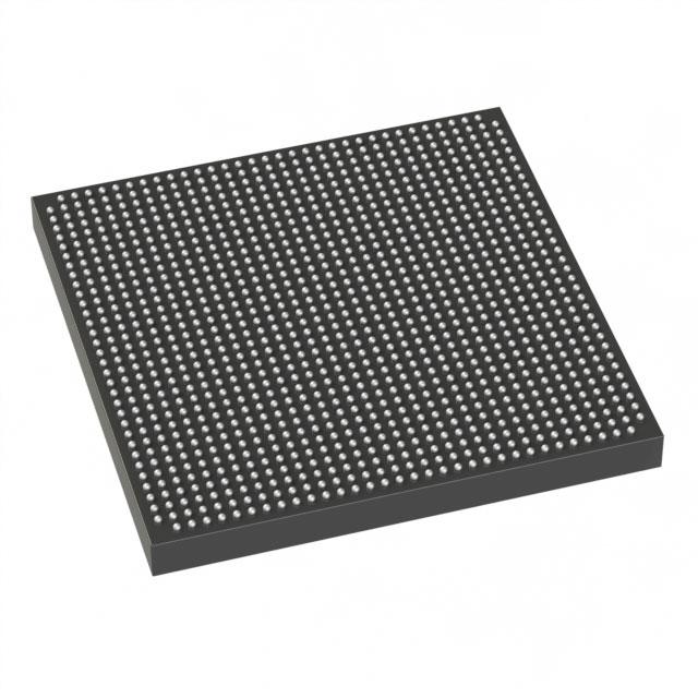
| Package / Case | 1152-BBGA, FCBGA | |
| Supplier Device Package | 1152-FBGA (35x35) | |
| Base Product Number | 5SGXEA3 |
5SGXEA3K2F35I3LN Datasheet Download
5SGXEA3K2F35I3LN Overview
The 5SGXEA3K2F35I3LN is an FPGA chip from Altera, a subsidiary of Intel. It is part of the Stratix V family and is based on the 28nm process. It features a total of 3,542,432 logic elements, 5,824 embedded memory blocks, and 1,152 18×18 multipliers. It has a total of 1,152 user I/Os and a total power consumption of up to 33.9W. The chip also has an integrated transceiver that supports up to 28.05Gbps data rates.
The 5SGXEA3K2F35I3LN is designed for a wide range of applications including high-end networking, computing, and storage. It is suitable for applications that require high levels of performance, such as high-speed networking, video processing, and data encryption. It is also suitable for applications that require high levels of integration, such as embedded systems and Internet of Things (IoT) devices.
The chip supports a wide range of protocols, including PCIe, Ethernet, SATA, USB, and HDMI. It also supports a wide range of I/O standards, such as LVDS, LVCMOS, and HCSL. The chip is also compatible with a wide range of software development tools, including Altera's Quartus II and Nios II software development kits.
In summary, the 5SGXEA3K2F35I3LN is an FPGA chip from Altera that is designed for a wide range of applications. It features a total of 3,542,432 logic elements, 5,824 embedded memory blocks, and 1,152 18×18 multipliers. It has a total of 1,152 user I/Os and a total power consumption of up to 33.9W. The chip also has an integrated transceiver that supports up to 28.05Gbps data rates. It supports a wide range of protocols and I/O standards, and is compatible with a wide range of software development tools.
You May Also Be Interested In

1,403 In Stock
Pricing (USD)
| QTY | Unit Price | Ext Price |
|---|---|---|
| No reference price found. | ||