

Intel Corporation
5SGSMD8K1F40I2N
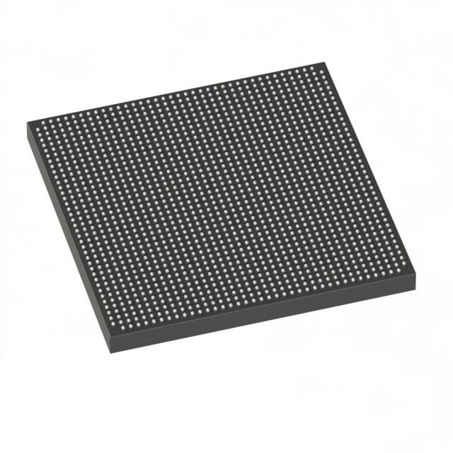
5SGSMD8K1F40I2N ECAD Model
5SGSMD8K1F40I2N Attributes
| Type | Description | Select |
|---|---|---|
| Mfr | Intel | |
| Series | Stratix® V GS | |
| Package | Tray | |
| Number of LABs/CLBs | 262400 | |
| Number of Logic Elements/Cells | 695000 | |
| Total RAM Bits | 51200000 | |
| Number of I/O | 696 | |
| Voltage - Supply | 0.87V ~ 0.93V | |
| Mounting Type | Surface Mount | |
| Operating Temperature | -40°C ~ 100°C (TJ) | |
| Package / Case | 1517-BBGA, FCBGA | |
| Supplier Device Package | 1517-FBGA (40x40) | |
| Base Product Number | 5SGSMD8 |
5SGSMD8K1F40I2N Datasheet Download
5SGSMD8K1F40I2N Overview
The 5SGSMD8K1F40I2N is an Altera Stratix V FPGA chip, part of the Cyclone V family. It is a high-end FPGA with 28,160 logic elements and 5.3 million system gates, making it suitable for a wide range of applications. It has a total of 8,192 Kbits of embedded memory and 8,192 Kbits of distributed memory. It also features a high-speed transceiver block with up to 28 channels of up to 28Gbps. It also features a high-speed serializer/deserializer (SERDES) block with up to 28 channels of up to 28Gbps.
The 5SGSMD8K1F40I2N is manufactured using a 40nm process technology, and has an operating temperature range of 0°C to 85°C. It has a total power consumption of up to 20W and a total of 456 user I/Os. It also features a JTAG interface for programming and debugging.
The 5SGSMD8K1F40I2N is suitable for a wide range of applications, including high-speed networking, video processing, embedded systems, and automotive applications. It is also suitable for applications that require high-performance, low-power, and high-reliability.
In conclusion, the 5SGSMD8K1F40I2N is a high-end FPGA from the Cyclone V family, suitable for a wide range of applications. It has a high-speed transceiver block, a serializer/deserializer block, and a JTAG interface. It is manufactured using a 40nm process technology, and has an operating temperature range of 0°C to 85°C. It has a total power consumption of up to 20W and a total of 456 user I/Os.
You May Also Be Interested In

3,464 In Stock
Pricing (USD)
| QTY | Unit Price | Ext Price |
|---|---|---|
| No reference price found. | ||