
Intel Corporation
10AX066K3F40I2SG
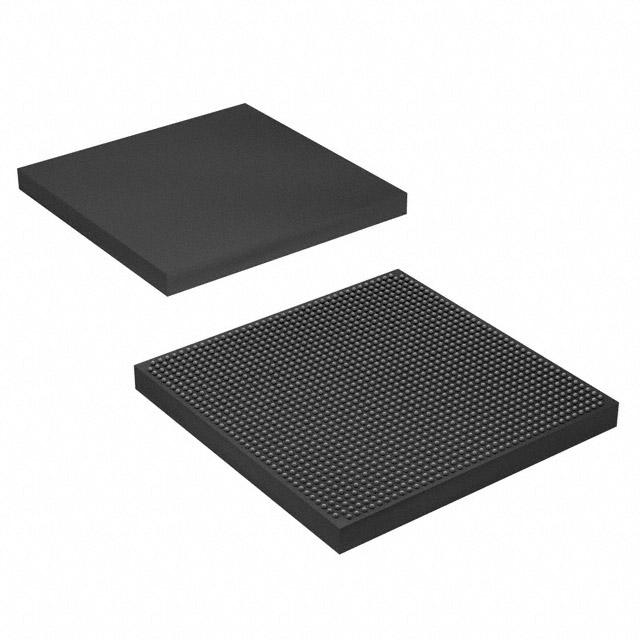
10AX066K3F40I2SG ECAD Model
10AX066K3F40I2SG Attributes
| Type | Description | Select |
|---|---|---|
| Rohs Code | Yes | |
| Part Life Cycle Code | Active | |
| Supply Voltage-Nom | 900 mV | |
| Number of Inputs | 696 | |
| Number of Outputs | 696 | |
| Number of Logic Cells | 660000 | |
| Number of CLBs | 25168 | |
| Programmable Logic Type | FIELD PROGRAMMABLE GATE ARRAY | |
| Temperature Grade | INDUSTRIAL | |
| Package Shape | SQUARE | |
| Technology | TSMC | |
| Organization | 25168 CLBS | |
| Additional Feature | ALSO OPERATES AT 0.95V NOMINAL SUPPLY | |
| Power Supplies | 900 mV | |
| Supply Voltage-Max | 930 mV | |
| Supply Voltage-Min | 870 mV | |
| JESD-30 Code | S-PBGA-B1517 | |
| Qualification Status | Not Qualified | |
| Operating Temperature-Max | 100 °C | |
| Operating Temperature-Min | -40 °C | |
| Peak Reflow Temperature (Cel) | NOT SPECIFIED | |
| Time@Peak Reflow Temperature-Max (s) | NOT SPECIFIED | |
| Number of Terminals | 1517 | |
| Package Body Material | PLASTIC/EPOXY | |
| Package Code | BGA | |
| Package Equivalence Code | BGA1517,39X39,40 | |
| Package Shape | SQUARE | |
| Package Style | GRID ARRAY | |
| Surface Mount | YES | |
| Terminal Form | BALL | |
| Terminal Pitch | 1 mm | |
| Terminal Position | BOTTOM | |
| Width | 40 mm | |
| Length | 40 mm | |
| Seated Height-Max | 3.5 mm | |
| Ihs Manufacturer | INTEL CORP | |
| Package Description | BGA, BGA1517,39X39,40 | |
| Reach Compliance Code | compliant | |
| HTS Code | 8542.39.00.01 |
10AX066K3F40I2SG Datasheet Download
10AX066K3F40I2SG Overview
The chip model 10AX066K3F40I2SG is an advanced integrated circuit designed for high-performance digital signal processing, embedded processing, and image processing. It is based on the Altera 10AX066K3F40I2SG technology, which is a field-programmable gate array (FPGA) device. This FPGA device contains a large number of programmable logic blocks, which can be used to implement complex digital designs.
The original design intention of the chip model 10AX066K3F40I2SG was to provide a powerful platform for digital signal processing, embedded processing, and image processing. It is designed to be used with the HDL language, which is a hardware description language (HDL) used to describe the behavior of digital systems. The chip model 10AX066K3F40I2SG also has the potential for future upgrades, as it can be used to implement advanced communication systems.
The product description of the chip model 10AX066K3F40I2SG includes its features, such as its high-speed performance, programmable logic blocks, and integrated 8-bit ADC and DAC. It also has a range of I/O options, such as USB, Ethernet, and RS-232. Furthermore, it is designed to be used with Altera's Quartus II design software, which provides a comprehensive set of design tools for creating digital designs.
Case studies and actual applications of the chip model 10AX066K3F40I2SG include its use in image processing, embedded systems, and high-performance digital signal processing. In addition, it can be used to implement advanced communication systems, such as wireless communication, satellite communication, and cellular communication.
When using the chip model 10AX066K3F40I2SG, it is important to take into account the power and thermal requirements of the device. Additionally, it is important to ensure that the design is compatible with the Altera Quartus II design software. Furthermore, the HDL code used to program the chip model 10AX066K3F40I2SG should be tested and verified before it is used in any application.
You May Also Be Interested In

5,945 In Stock
Pricing (USD)
| QTY | Unit Price | Ext Price |
|---|---|---|
| 1+ | $3,022.8769 | $3,022.8769 |
| 10+ | $2,990.3729 | $29,903.7288 |
| 100+ | $2,827.8526 | $282,785.2611 |
| 1000+ | $2,665.3323 | $1,332,666.1730 |
| 10000+ | $2,437.8040 | $2,437,803.9750 |
| The price is for reference only, please refer to the actual quotation! | ||