
Altera Corporation
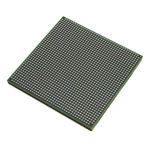
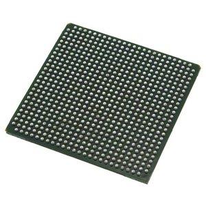
EP4S100G2F40C2N
EP4S100G2F40C2N ECAD Model
EP4S100G2F40C2N Attributes
| Type | Description | Select |
|---|---|---|
| Part Life Cycle Code | Transferred | |
| Number of CLBs | 91200 | |
| Programmable Logic Type | FIELD PROGRAMMABLE GATE ARRAY | |
| Temperature Grade | OTHER | |
| Package Shape | SQUARE | |
| Organization | 91200 CLBS | |
| JESD-30 Code | S-PBGA-B | |
| Operating Temperature-Max | 85 °C | |
| Number of Terminals | 1517 | |
| Package Body Material | PLASTIC/EPOXY | |
| Package Code | BGA | |
| Package Shape | SQUARE | |
| Package Style | GRID ARRAY | |
| Surface Mount | YES | |
| Terminal Form | BALL | |
| Terminal Pitch | 1 mm | |
| Terminal Position | BOTTOM | |
| Width | 40 mm | |
| Length | 40 mm | |
| Seated Height-Max | 3.8 mm | |
| Ihs Manufacturer | ALTERA CORP | |
| Part Package Code | BGA | |
| Package Description | BGA, | |
| Pin Count | 1517 | |
| Reach Compliance Code | unknown | |
| HTS Code | 8542.39.00.01 |
EP4S100G2F40C2N Datasheet Download
EP4S100G2F40C2N Overview
The chip model EP4S100G2F40C2N is a high-performance, low-power FPGA chip that is suitable for a wide range of applications, including high-performance digital signal processing, embedded processing, image processing, and more. It is designed to be used with the HDL language, allowing users to quickly and easily create a variety of applications.
The EP4S100G2F40C2N has a number of advantages that make it an attractive option for many industries. It is designed to be low-power, allowing it to be used in energy-efficient systems. It is also highly flexible, allowing it to be used in a variety of applications. Additionally, it is designed to be highly scalable and customizable, allowing it to be used in a variety of applications, from simple projects to complex ones.
The EP4S100G2F40C2N is expected to be in high demand in the future, as its low-power design and scalability make it a great choice for many industries. In particular, its flexibility and customizability make it ideal for use in advanced communication systems, such as 5G networks. Additionally, its scalability and customizability make it a great choice for use in embedded systems and image processing.
The original design intention of the EP4S100G2F40C2N was to create a low-power, highly flexible FPGA chip that could be used in a variety of applications. The chip was designed to be highly scalable and customizable, allowing users to create a variety of applications with relative ease. Additionally, the chip was designed to be used with the HDL language, allowing users to quickly and easily create a variety of applications.
The EP4S100G2F40C2N is designed to be highly upgradable, allowing users to easily upgrade the chip to use new technologies and features. This makes it an attractive option for use in advanced communication systems as it can be easily upgraded to use new technologies. Additionally, its scalability and customizability make it a great choice for use in embedded systems and image processing.
Overall, the EP4S100G2F40C2N is a great choice for a variety of applications. Its low-power design and scalability make it an attractive option for many industries. Additionally, its flexibility and customizability make it ideal for use in advanced communication systems, as well as embedded systems and image processing. Finally, its upgradability makes it a great choice for use in advanced communication systems, as it can be easily upgraded to use new technologies.
You May Also Be Interested In
3,077 In Stock
Pricing (USD)
| QTY | Unit Price | Ext Price |
|---|---|---|
| 1+ | $123.2585 | $123.2585 |
| 10+ | $121.9331 | $1,219.3312 |
| 100+ | $115.3063 | $11,530.6320 |
| 1000+ | $108.6795 | $54,339.7600 |
| 10000+ | $99.4020 | $99,402.0000 |
| The price is for reference only, please refer to the actual quotation! | ||