
Altera Corporation
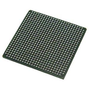
EP2SGX90EF35C5NES
EP2SGX90EF35C5NES ECAD Model
EP2SGX90EF35C5NES Attributes
| Type | Description | Select |
|---|---|---|
| Pbfree Code | Yes | |
| Rohs Code | Yes | |
| Part Life Cycle Code | Transferred | |
| Supply Voltage-Nom | 1.2 V | |
| Number of CLBs | 4828 | |
| Programmable Logic Type | FIELD PROGRAMMABLE GATE ARRAY | |
| Temperature Grade | COMMERCIAL EXTENDED | |
| Package Shape | SQUARE | |
| Technology | CMOS | |
| Organization | 4828 CLBS | |
| Supply Voltage-Max | 1.25 V | |
| Supply Voltage-Min | 1.15 V | |
| JESD-30 Code | S-PBGA-B35 | |
| Qualification Status | Not Qualified | |
| JESD-609 Code | e1 | |
| Operating Temperature-Max | 85 °C | |
| Number of Terminals | 35 | |
| Package Body Material | PLASTIC/EPOXY | |
| Package Code | BGA | |
| Package Shape | SQUARE | |
| Package Style | GRID ARRAY | |
| Surface Mount | YES | |
| Terminal Finish | TIN SILVER COPPER | |
| Terminal Form | BALL | |
| Terminal Position | BOTTOM | |
| Ihs Manufacturer | ALTERA CORP | |
| Part Package Code | PGA | |
| Package Description | BGA, | |
| Pin Count | 35 | |
| Reach Compliance Code | compliant | |
| HTS Code | 8542.39.00.01 |
EP2SGX90EF35C5NES Datasheet Download
EP2SGX90EF35C5NES Overview
The chip model EP2SGX90EF35C5NES is a high-performance, low-power FPGA (Field Programmable Gate Array) designed for digital signal processing, embedded processing and image processing applications. It is designed to be used with HDL (Hardware Description Language) and is capable of delivering high performance and low power consumption.
The EP2SGX90EF35C5NES offers several advantages over other FPGA models. It has a large capacity of up to 90,000 logic elements and 4,000Kbits of embedded memory, making it suitable for complex applications. It also features a low-power architecture, which helps reduce power consumption while maintaining performance. Additionally, the chip model is designed to be flexible, allowing developers to customize the design to meet their specific needs.
The demand for the EP2SGX90EF35C5NES chip model is expected to grow in the future, as more industries become dependent on digital signal processing, embedded processing and image processing applications. The chip model's low-power architecture, high performance and flexible design make it an attractive option for these industries.
When designing products with the EP2SGX90EF35C5NES chip model, it is important to consider the specific design requirements of the application. This includes the number of logic elements needed, the type of memory required and the power requirements of the system. Additionally, it is important to consider any potential issues that could arise with the design, such as timing constraints or signal integrity.
In order to ensure the successful implementation of the EP2SGX90EF35C5NES chip model, it is important to study actual case studies and take precautions to avoid potential issues. For example, developers should familiarize themselves with the HDL language used to program the chip model and the design process for the application. Additionally, it is important to test the design thoroughly and make sure that all components are working properly.
Overall, the EP2SGX90EF35C5NES chip model is an attractive option for digital signal processing, embedded processing and image processing applications. With its low-power architecture, high performance and flexible design, the chip model is expected to become increasingly popular in the future. When designing products with the chip model, it is important to consider the specific design requirements of the application and take precautions to ensure the successful implementation of the chip model.
You May Also Be Interested In

3,733 In Stock
Pricing (USD)
| QTY | Unit Price | Ext Price |
|---|---|---|
| No reference price found. | ||