
Altera Corporation
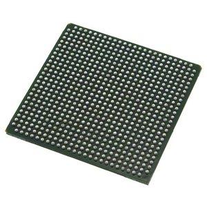
EP2SGX90EF35C4NES
EP2SGX90EF35C4NES ECAD Model
EP2SGX90EF35C4NES Attributes
| Type | Description | Select |
|---|---|---|
| Pbfree Code | Yes | |
| Rohs Code | Yes | |
| Part Life Cycle Code | Transferred | |
| Supply Voltage-Nom | 1.2 V | |
| Number of CLBs | 4828 | |
| Programmable Logic Type | FIELD PROGRAMMABLE GATE ARRAY | |
| Temperature Grade | COMMERCIAL EXTENDED | |
| Package Shape | SQUARE | |
| Technology | CMOS | |
| Organization | 4828 CLBS | |
| Supply Voltage-Max | 1.25 V | |
| Supply Voltage-Min | 1.15 V | |
| JESD-30 Code | S-PBGA-B35 | |
| Qualification Status | Not Qualified | |
| JESD-609 Code | e1 | |
| Operating Temperature-Max | 85 °C | |
| Number of Terminals | 35 | |
| Package Body Material | PLASTIC/EPOXY | |
| Package Code | BGA | |
| Package Shape | SQUARE | |
| Package Style | GRID ARRAY | |
| Surface Mount | YES | |
| Terminal Finish | TIN SILVER COPPER | |
| Terminal Form | BALL | |
| Terminal Position | BOTTOM | |
| Ihs Manufacturer | ALTERA CORP | |
| Part Package Code | PGA | |
| Package Description | BGA, | |
| Pin Count | 35 | |
| Reach Compliance Code | compliant | |
| HTS Code | 8542.39.00.01 |
EP2SGX90EF35C4NES Datasheet Download
EP2SGX90EF35C4NES Overview
The chip model EP2SGX90EF35C4NES is a high performance digital signal processing (DSP) chip developed by Altera. It is designed to meet the needs of embedded processing, image processing and other applications. This chip is based on the Stratix II GX FPGA technology and uses HDL language for its programming.
The product description of the chip model EP2SGX90EF35C4NES includes its features and specifications. It has a total of up to 90K logic elements, up to 1.2 million bits of embedded memory and up to 9.6Gbps of total transceiver bandwidth. It also has a wide variety of I/O options, including LVDS, SSTL and multi-gigabit transceivers. In addition, it has a power-saving design and supports the use of hot-swappable memory modules.
When using the chip model EP2SGX90EF35C4NES, there are certain design requirements that must be met. For example, the signal integrity must be considered when designing the board layout. Also, the clock signal must be synchronized with the data signals and the power supply must be stable. In addition, the timing of the FPGA must be verified to ensure that it is operating correctly.
There are several case studies that demonstrate the effectiveness of the chip model EP2SGX90EF35C4NES. For example, it has been used for image processing in robotics applications. It has also been used for high-speed communications and for the development of intelligent robots. In addition, it has been used for the development of embedded systems and for the development of medical imaging systems.
The chip model EP2SGX90EF35C4NES can be used in the development and popularization of future intelligent robots. It can be used to process data quickly and accurately, as well as to control the robot's movements. In order to use the chip model EP2SGX90EF35C4NES effectively, technical talents such as engineers and computer scientists are needed. They should be familiar with HDL language and should have knowledge of signal processing, embedded systems and robotics.
In conclusion, the chip model EP2SGX90EF35C4NES is a high performance digital signal processing chip that is suitable for a variety of applications. It has a variety of features and specifications and requires certain design considerations when using it. It can be used in the development and popularization of future intelligent robots, and technical talents are needed to use it effectively.
You May Also Be Interested In

1,726 In Stock
Pricing (USD)
| QTY | Unit Price | Ext Price |
|---|---|---|
| No reference price found. | ||