

Altera Corporation
EP2S15F484I5
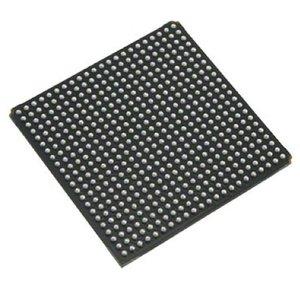
EP2S15F484I5 ECAD Model
EP2S15F484I5 Attributes
| Type | Description | Select |
|---|---|---|
| Rohs Code | No | |
| Part Life Cycle Code | Transferred | |
| Number of Inputs | 342 | |
| Number of Outputs | 334 | |
| Number of Logic Cells | 15600 | |
| Programmable Logic Type | FIELD PROGRAMMABLE GATE ARRAY | |
| Package Shape | SQUARE | |
| Technology | CMOS | |
| Power Supplies | 1.2,1.5/3.3,3.3 V | |
| JESD-30 Code | S-PBGA-B484 | |
| Qualification Status | Not Qualified | |
| JESD-609 Code | e0 | |
| Moisture Sensitivity Level | 3 | |
| Peak Reflow Temperature (Cel) | 220 | |
| Number of Terminals | 484 | |
| Package Body Material | PLASTIC/EPOXY | |
| Package Code | BGA | |
| Package Equivalence Code | BGA484,22X22,40 | |
| Package Shape | SQUARE | |
| Package Style | GRID ARRAY | |
| Surface Mount | YES | |
| Terminal Finish | TIN LEAD | |
| Terminal Form | BALL | |
| Terminal Pitch | 1 mm | |
| Terminal Position | BOTTOM | |
| Ihs Manufacturer | ALTERA CORP | |
| Package Description | BGA, BGA484,22X22,40 | |
| Reach Compliance Code | compliant | |
| HTS Code | 8542.39.00.01 |
EP2S15F484I5 Datasheet Download
EP2S15F484I5 Overview
The chip model EP2S15F484I5 is a high-performance field programmable gate array (FPGA) designed by Altera Corporation. It is a member of the Stratix II family and has a capacity of up to 15 million logic elements. It has a wide range of applications in the fields of communications, industrial control, consumer electronics, and so on.
In recent years, the chip model EP2S15F484I5 has seen increasing demand in the market due to its high performance and low power consumption. With the rapid development of the Internet of Things (IoT) and artificial intelligence (AI), the chip model EP2S15F484I5 is expected to be widely used in networks, intelligent scenarios, and fully intelligent systems.
The chip model EP2S15F484I5 is designed with a number of features that make it suitable for a variety of applications. It supports a range of I/O standards including LVDS, LVCMOS, and SSTL. It also supports a wide range of clock frequencies from 33MHz to 200MHz. As a result, the chip model EP2S15F484I5 can be used in a variety of applications that require high performance and low power consumption.
In addition, the chip model EP2S15F484I5 has a number of advanced features that make it suitable for use in intelligent scenarios. It supports a range of communication protocols such as Ethernet, USB, and CAN. It also supports a wide range of memory types including SRAM, DRAM, and Flash. As a result, the chip model EP2S15F484I5 can be used in a variety of applications that require high-speed communication and data storage.
When designing with the chip model EP2S15F484I5, it is important to consider the specific requirements of the application. For example, the power consumption of the chip model EP2S15F484I5 should be taken into account when designing for applications that require low power consumption. Similarly, the communication protocols and memory types should be considered when designing for applications that require high-speed communication and data storage.
In conclusion, the chip model EP2S15F484I5 is a high-performance FPGA with a wide range of applications. It is expected to be widely used in networks, intelligent scenarios, and fully intelligent systems in the future. When designing with the chip model EP2S15F484I5, it is important to consider the specific requirements of the application and take into account the power consumption, communication protocols, and memory types.
You May Also Be Interested In
3,816 In Stock
Pricing (USD)
| QTY | Unit Price | Ext Price |
|---|---|---|
| No reference price found. | ||