
Altera Corporation
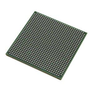
EP2C70F896I7N
EP2C70F896I7N ECAD Model
EP2C70F896I7N Attributes
| Type | Description | Select |
|---|---|---|
| Pbfree Code | Yes | |
| Rohs Code | Yes | |
| Part Life Cycle Code | Transferred | |
| Supply Voltage-Nom | 1.2 V | |
| Number of Inputs | 622 | |
| Number of Outputs | 606 | |
| Number of Logic Cells | 68416 | |
| Number of CLBs | 4300 | |
| Programmable Logic Type | FIELD PROGRAMMABLE GATE ARRAY | |
| Package Shape | SQUARE | |
| Technology | CMOS | |
| Organization | 4300 CLBS | |
| Additional Feature | ALSO REQUIRES 3.3 SUPPLY | |
| Power Supplies | 1.2,1.5/3.3,3.3 V | |
| Supply Voltage-Max | 1.25 V | |
| Supply Voltage-Min | 1.15 V | |
| JESD-30 Code | S-PBGA-B896 | |
| Qualification Status | Not Qualified | |
| JESD-609 Code | e1 | |
| Number of Terminals | 896 | |
| Package Body Material | PLASTIC/EPOXY | |
| Package Code | BGA | |
| Package Equivalence Code | BGA896,30X30,40 | |
| Package Shape | SQUARE | |
| Package Style | GRID ARRAY | |
| Surface Mount | YES | |
| Terminal Finish | TIN SILVER COPPER | |
| Terminal Form | BALL | |
| Terminal Pitch | 1 mm | |
| Terminal Position | BOTTOM | |
| Width | 31 mm | |
| Length | 31 mm | |
| Seated Height-Max | 2.6 mm | |
| Ihs Manufacturer | ALTERA CORP | |
| Part Package Code | BGA | |
| Package Description | BGA, BGA896,30X30,40 | |
| Pin Count | 896 | |
| Reach Compliance Code | compliant | |
| HTS Code | 8542.39.00.01 |
EP2C70F896I7N Datasheet Download
EP2C70F896I7N Overview
The chip model EP2C70F896I7N is a high-performance, low-power FPGA developed by Altera Corporation. It is designed to provide a reliable and cost-effective solution for a wide range of applications, including consumer electronics, medical devices, industrial automation, automotive, and aerospace.
The EP2C70F896I7N is based on the 28nm technology process and integrates a variety of high-performance components, including a 4-Gigabit DDR3 memory controller, a PCI Express Gen3 x8 interface, and a high-speed transceiver. It also provides various I/O and logic functions, such as LVDS, SERDES, HDMI, and Gigabit Ethernet.
The EP2C70F896I7N is designed to meet the requirements of advanced communication systems, such as 5G, LTE, and Wi-Fi. It is also suitable for applications that require high-speed data processing, such as video streaming, image processing, and machine learning. In addition, the chip model is designed to be highly scalable and can be upgraded to meet the changing demands of applications.
The EP2C70F896I7N has a wide range of applications, such as machine vision, medical imaging, and industrial automation. In order to ensure the safety and reliability of the chip model, it is necessary to pay attention to the specific design requirements of the chip model, such as power consumption, temperature, and EMI.
In conclusion, the chip model EP2C70F896I7N is a reliable and cost-effective solution for a wide range of applications. It is designed to meet the requirements of advanced communication systems and is highly scalable. In order to ensure the safety and reliability of the chip model, it is necessary to pay attention to the specific design requirements of the chip model.
You May Also Be Interested In

1,430 In Stock
Pricing (USD)
| QTY | Unit Price | Ext Price |
|---|---|---|
| 1+ | $379.4400 | $379.4400 |
| 10+ | $375.3600 | $3,753.6000 |
| 100+ | $354.9600 | $35,496.0000 |
| 1000+ | $334.5600 | $167,280.0000 |
| 10000+ | $306.0000 | $306,000.0000 |
| The price is for reference only, please refer to the actual quotation! | ||